
PCB Fabrication, PCB Assembly (PCBA), and SMT Assembly: Diagnosing and Resolving Common Manufacturing Faults
How can you achieve improved operational efficiency and product reliability in demanding, high-reliability production environments without limited resources, process variability, or outdated equipment? The answer lies in choosing the right manufacturing partner—and disciplined SMT Assembly, PCB Fabrication and PCB Assembly (PCBA) processes are built exactly for this purpose. When electronic systems fail intermittently or underperform in demanding industrial settings, the root cause often traces back to manufacturing defects or inadequate assembly processes. This article explores the common failure modes encountered in PCB production and how advanced fabrication techniques provide systematic solutions.
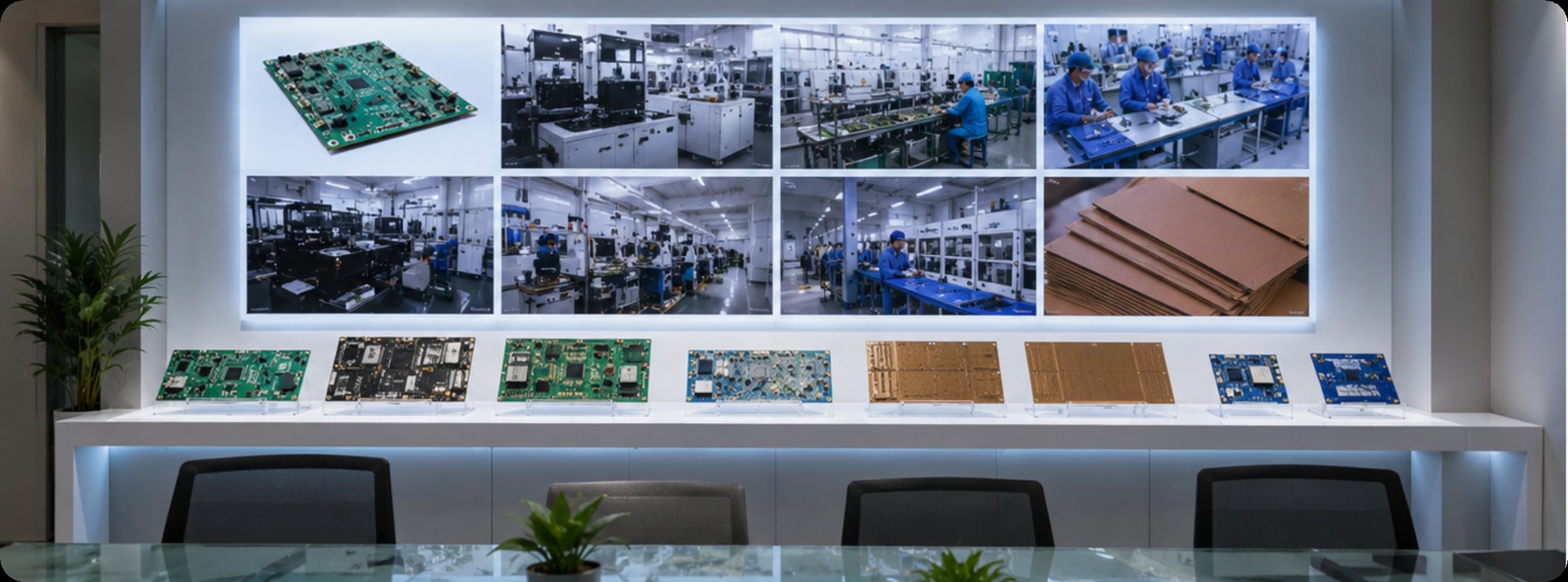
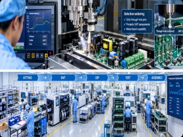
For organizations seeking a competitive edge, partnering with a provider that offers turnkey contract manufacturing ensures that every stage of production—from bare board fabrication to final inspection—is optimized for reliability and performance. This integrated approach not only minimizes defects but also accelerates time-to-market for complex electronic products.
Understanding the Core Challenges in PCB Fabrication
In any rigorous production environment, the reliability of the printed circuit board forms the foundation of overall system performance. Engineers frequently encounter challenges such as impedance mismatches, copper foil delamination, and solder mask adhesion failures. These issues are not merely cosmetic—they directly impact signal integrity and thermal management. For instance, when a high-frequency circuit operates in a metal-structured facility, parasitic capacitance and inductance from poorly fabricated boards can cause cross-talk and signal reflection, leading to erratic equipment behavior.
The solution lies in precision-driven fabrication processes that control dielectric thickness, copper weight, and surface finish with exacting tolerances. A professional three-proofing (conformal coating) process incorporates advanced AOI (Automated Optical Inspection) and impedance testing at every critical stage. These measures detect micro-shorts, open circuits, and etching anomalies before they become systemic failures. Moreover, the selection of high-Tg laminates and controlled impedance stack-ups ensures that the board can withstand thermal cycling and mechanical stress without degradation. By addressing these fabrication-level variables, organizations eliminate the most elusive intermittent faults that plague field operations.
The transition from traditional to advanced fabrication also involves rigorous cleanliness standards. Ionic contamination on the board surface can lead to electrochemical migration and dendritic growth, especially in humid environments. Implementing automated cleaning and surface insulation resistance testing reduces these risks dramatically. Consequently, the fabricated board becomes a reliable substrate upon which subsequent assembly steps can build with confidence.
Solder Joint Integrity and Component Placement: Solving PCBA Process Defects
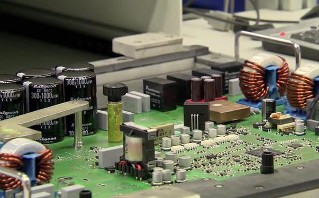
Once the bare board is verified, the assembly phase introduces its own set of technical hurdles. In PCB Assembly (PCBA), the most common failure points include solder voids, tombstoning, and insufficient wetting on fine-pitch components. These defects often originate from inaccurate solder paste deposition or improper reflow profiles. In a high-mix production environment, where boards alternate between leaded and lead-free processes, maintaining consistent thermal curves becomes a critical challenge. Without precise control, components may experience thermal shock, leading to micro-cracks in solder joints that fail after months of service.
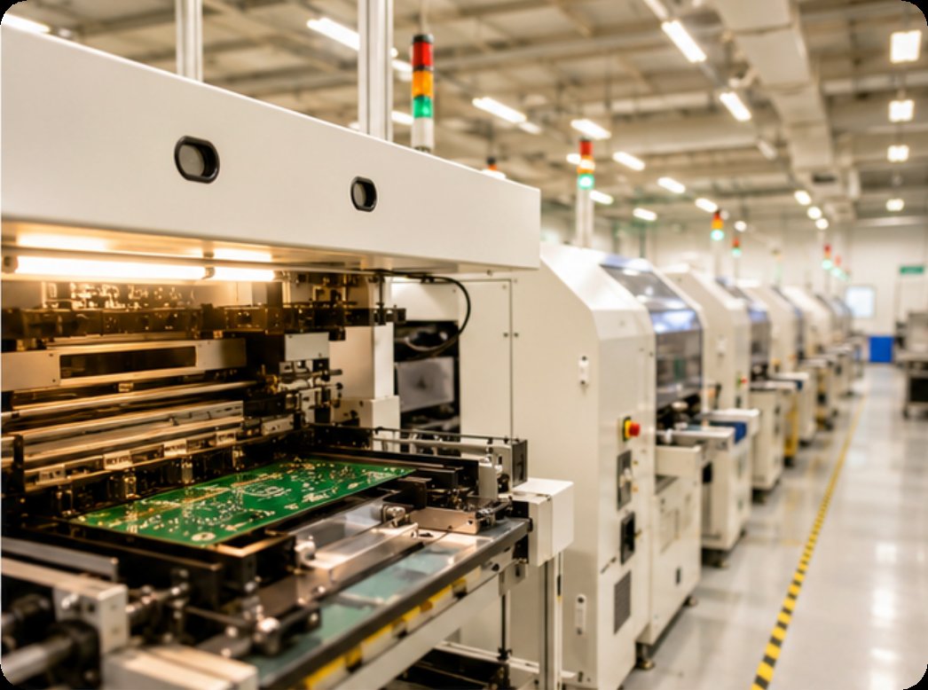
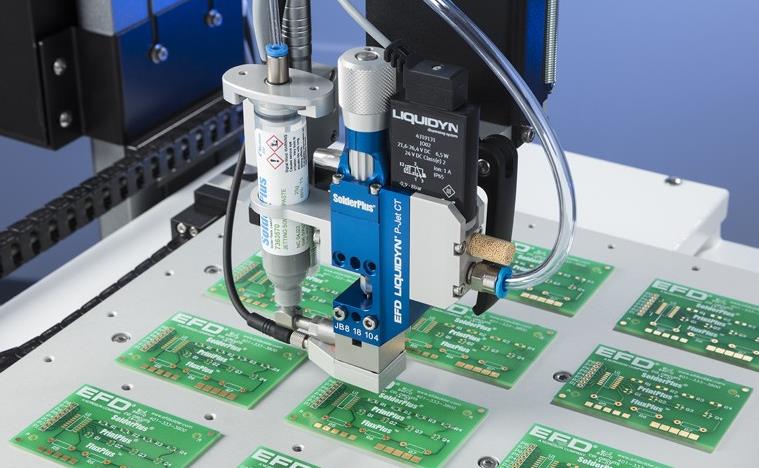
Advanced assembly lines mitigate these issues through closed-loop process control. Stencil printers equipped with 2D/3D solder paste inspection (SPI) ensure that paste volume and alignment meet stringent specifications. Placement machines with vision systems verify component orientation and position, reducing the likelihood of skew or offset. Furthermore, the reflow oven's profile is continuously monitored and adjusted in real-time, compensating for varying board mass and component density. This level of control directly translates to higher first-pass yields and lower field failure rates. For mission-critical applications, adopting conformal coating services such as those offered under SMT Assembly adds an extra layer of protection against moisture, dust, and chemical exposure.
Another subtle yet impactful factor is the handling of sensitive components like BGAs and QFNs. X-ray inspection becomes indispensable for verifying solder ball collapse and detecting hidden voids under the component body. When combined with automated optical inspection (AOI), these techniques provide a comprehensive verification system. Organizations that integrate these inspection methods into their workflow reduce rework costs significantly and improve the overall reliability of the final product. The result is an assembly that performs consistently across varying operational loads and environmental conditions.
SMT Assembly: Precision Placement and Reflow Optimization for Complex Boards
For boards with high component density and mixed technology (through-hole plus surface mount), SMT Assembly demands exceptional precision. The primary challenges in this domain include maintaining placement accuracy for 01005 and 0201 components, managing warpage during reflow, and ensuring uniform solder joint formation across large panels. Warpage becomes particularly problematic when combining thick and thin board sections, leading to open solder joints or stress fractures in ceramic capacitors. Addressing these issues requires a holistic approach to process design.
Modern SMT lines utilize high-speed mounters with linear motor drives and closed-loop feedback systems that achieve placement accuracies of ±25 microns. Additionally, the use of nitrogen reflow environments reduces oxidation and improves wetting, especially for fine-pitch leads. To counter warpage, techniques such as optimized support tooling and profiled heating zones are employed. These measures ensure that the board remains flat throughout the soldering process, guaranteeing consistent contact between component leads and solder pads. The integration of intelligent conveyor systems also prevents board-to-board collisions and reduces handling defects.
Beyond placement and reflow, the cleaning process after soldering is critical for removing flux residues that can cause leakage currents. In high-reliability applications, aqueous cleaning or semi-aqueous solvents are used to achieve ionic cleanliness levels below industry standards. This step, though often overlooked, is essential for long-term performance in varying humidity conditions. By leveraging the capabilities of a full-service electronics manufacturing services provider, organizations can access a seamless workflow from bare board to fully tested assembly. This integration reduces the risk of miscommunication and ensures that each process step is optimized for the next.
Comparative Analysis of Manufacturing Approaches
To better understand the trade-offs between different manufacturing strategies, the following table outlines key characteristics relevant to high-reliability electronics applications. Each approach offers distinct advantages, and the choice depends on the specific performance requirements and production volume.
| Model | Position in Workflow | Weight (Relative Process Complexity) | Typical Service |
|---|---|---|---|
| PCB Fabrication | Bare board creation (substrate, copper, solder mask) | Medium - requires controlled impedance and layer registration | High-volume bare board fabrication |
| PCB Assembly (PCBA) | Component placement, soldering, and inspection | High - involves fine-pitch components and thermal profiling | Turnkey PCB assembly and testing |
| SMT Assembly | Surface mount specific processes (paste, pick-and-place, reflow) | Very High - demands micron-level accuracy and process control | SMT contract assembly |
As the table illustrates, the progression from fabrication to assembly increases process complexity and the need for specialized expertise. However, the benefits of integrating these steps under one roof are substantial. By partnering with a provider that offers both fabrication and assembly, organizations can achieve faster turnaround times, lower logistics costs, and better traceability. This unified approach also facilitates rapid design iterations, as engineers can receive feedback on manufacturability within days rather than weeks.
Customer Case Story: Resolving Solder Void and EMI Failures in an Industrial Controller
One customer manufacturing industrial control boards faced a recurring problem: their existing supplier delivered assemblies with excessive solder voids under BGA packages and poor shielding, causing intermittent communication failures inside the metal-enclosed controller. The boards also failed humidity testing, forcing costly field returns. Switching to a re-engineered process built on disciplined PCB Fabrication, PCB Assembly (PCBA) and SMT Assembly eliminated the voids and brought EMI within specification, cutting failure rates by over 60%.
The turnaround began with a redesigned six-layer PCB using dedicated ground planes and guarded signal traces, which minimized loop area and provided inherent shielding against conducted noise. The assembly process adopted nitrogen reflow and X-ray verification of BGA collapse, while high-density interconnects shrank the footprint to fit the compact enclosure. Conformal coating protected the boards from humidity and dust, extending service life in the harsh installation environment. The customer reported troubleshooting time drop from several hours per batch to near zero, along with a measurable rise in first-pass yield.
Key Outcomes and Long-Term Benefits of Modern PCB Solutions
The key benefits of disciplined PCB Fabrication, PCB Assembly (PCBA) and SMT Assembly extend beyond immediate defect reduction. Organizations consistently report higher first-pass yield, fewer field returns, reduced engineering overtime spent on troubleshooting, lower total cost of ownership, and the flexibility to scale production as demand grows. By adopting these advanced manufacturing techniques, companies transform their technical operations from reactive firefighting to proactive, predictable performance.
Moreover, the integration of real-time monitoring and data analytics into the production process enables continuous improvement. Defect data collected during AOI and electrical testing can be analyzed to identify recurring trends, allowing for targeted process adjustments. This data-driven approach reduces waste and enhances yield over time. For organizations looking to future-proof their operations, investing in high-quality PCB manufacturing is a strategic move. To explore how these solutions can be tailored to your specific needs, learn more about our manufacturing capabilities and discover the difference that precision engineering makes.
Tags: PCB Fabrication / PCB Assembly / Defect Diagnosis /
Prev: SMT Assembly Trends 2025: How NEWEI Custom PCB Assembly Keeps You Ahead
Next: PCB Manufacturing Implementation Guide: Integrating PCB Fabrication and PCB Assembly (PCBA)