
From Tooling to Automotive Grade: How Shell Mold and DIP Assembly Evolved With PCB Manufacturing
The biggest mistake hardware buyers and engineering leads make is treating PCB manufacturing as a static menu of isolated options. In reality, modern electronic manufacturing services (EMS) keep evolving rapidly. Over the past decade, the traditional barrier between rapid prototyping and certified volume production has collapsed, driven by major advancements in three core capabilities: advanced PCB fabrication, custom enclosure production, and hybrid component assembly methods. If you benchmark your manufacturing partner solely on price per point, you overlook the exact operational efficiencies that determine your true time to market.
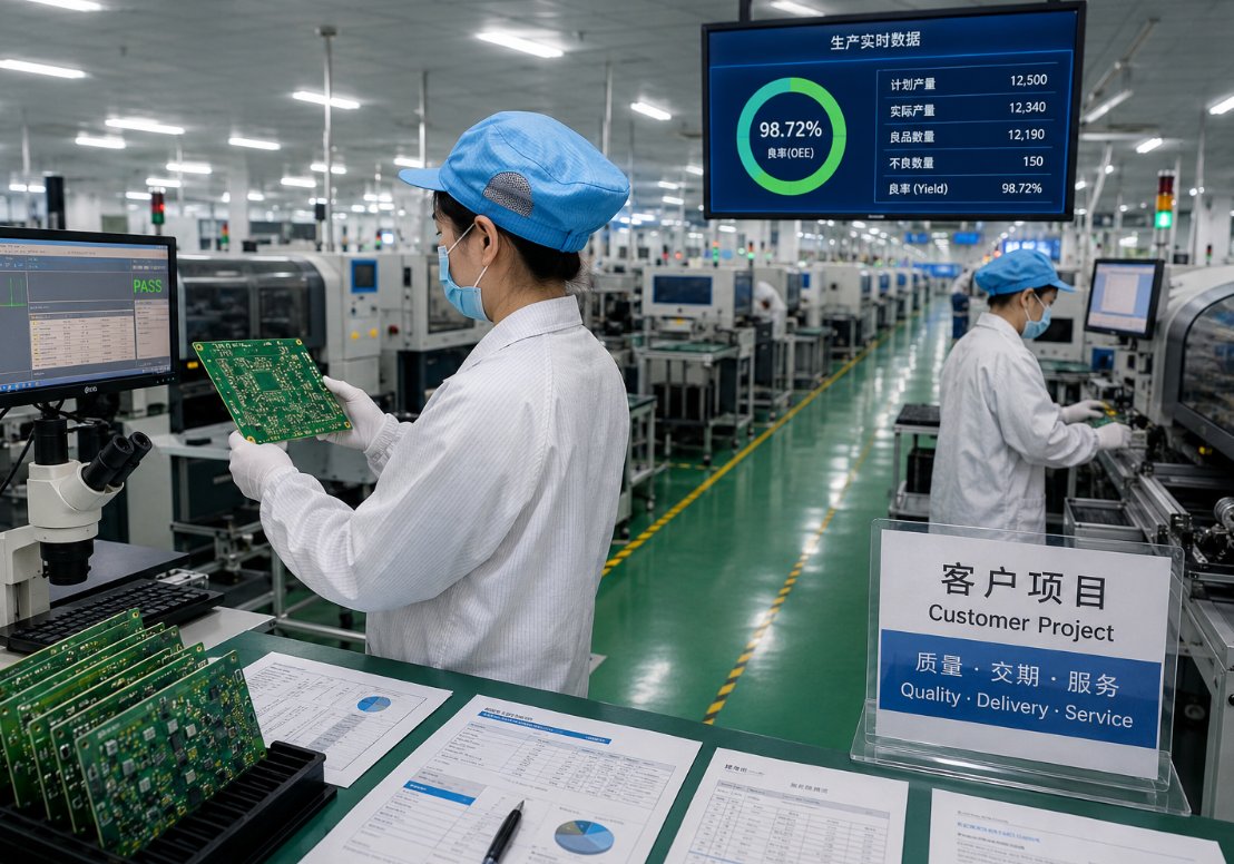
Our core perspective: market leaders are not defined merely by owning the newest machinery, but by their ability to execute shell mold enclosures, DIP assembly for robust through-hole components, and automotive-grade PCBA under a single roof without vendor handoffs. True innovation in electronics manufacturing is about eliminating handoff friction between steps, not relying on any single isolated process.
The Quiet Reset in Advanced PCB Manufacturing Capabilities
Throughout the 2000s, bringing a new electronic device to market meant navigating fragmented supply chains: a bare board fabricator produced the PCB, a separate contract manufacturer handled surface-mount stuffing, an external industrial designer molded the plastic casing, and a specialized testing house managed automotive certifications if required. That era of heavy separation is entirely gone. Today's advanced manufacturing capabilities operate on a unified digital thread, allowing individual processes to upgrade continuously while maintaining synchronized workflows.
The following analysis explores three vital tracks of this industrial evolution. While none represent headline-grabbing hype, together they determine whether your hardware build ships in three weeks or three months, and whether your finished product survives extreme thermal environments in the field or high-vibration industrial factory floors.
Shell Mold Enclosures: Faster Iteration, Finer Walls
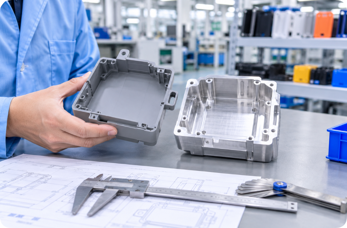
Historically, shell mold and custom enclosure prototyping required machining a costly aluminum prototype followed by an extended wait for hard steel injection tooling. The enclosure was invariably the slowest bottleneck in early-stage projects, forcing design teams to freeze mechanical geometry long before electronic schematics were finalized. That bottleneck has largely disappeared. Modern Shell Mold techniques utilize advanced silicone tooling printed or cast in days rather than weeks, achieving wall tolerances previously impossible with soft tooling.
This evolution extends far beyond raw speed. Finer wall thicknesses allow compact enclosures to house sophisticated circuit boards, a critical advantage for wearable electronics, handheld devices, and portable test equipment. We routinely integrate functional living hinges, complex snap-fit features, and custom textured surfaces directly into shell mold enclosures—features that once demanded expensive production-grade hard tooling. For low- to mid-volume production runs, the economic model has completely shifted: investing heavily in hard injection tooling upfront is now the exception rather than the rule.
DIP Assembly: The Through-Hole Track That Refused to Die
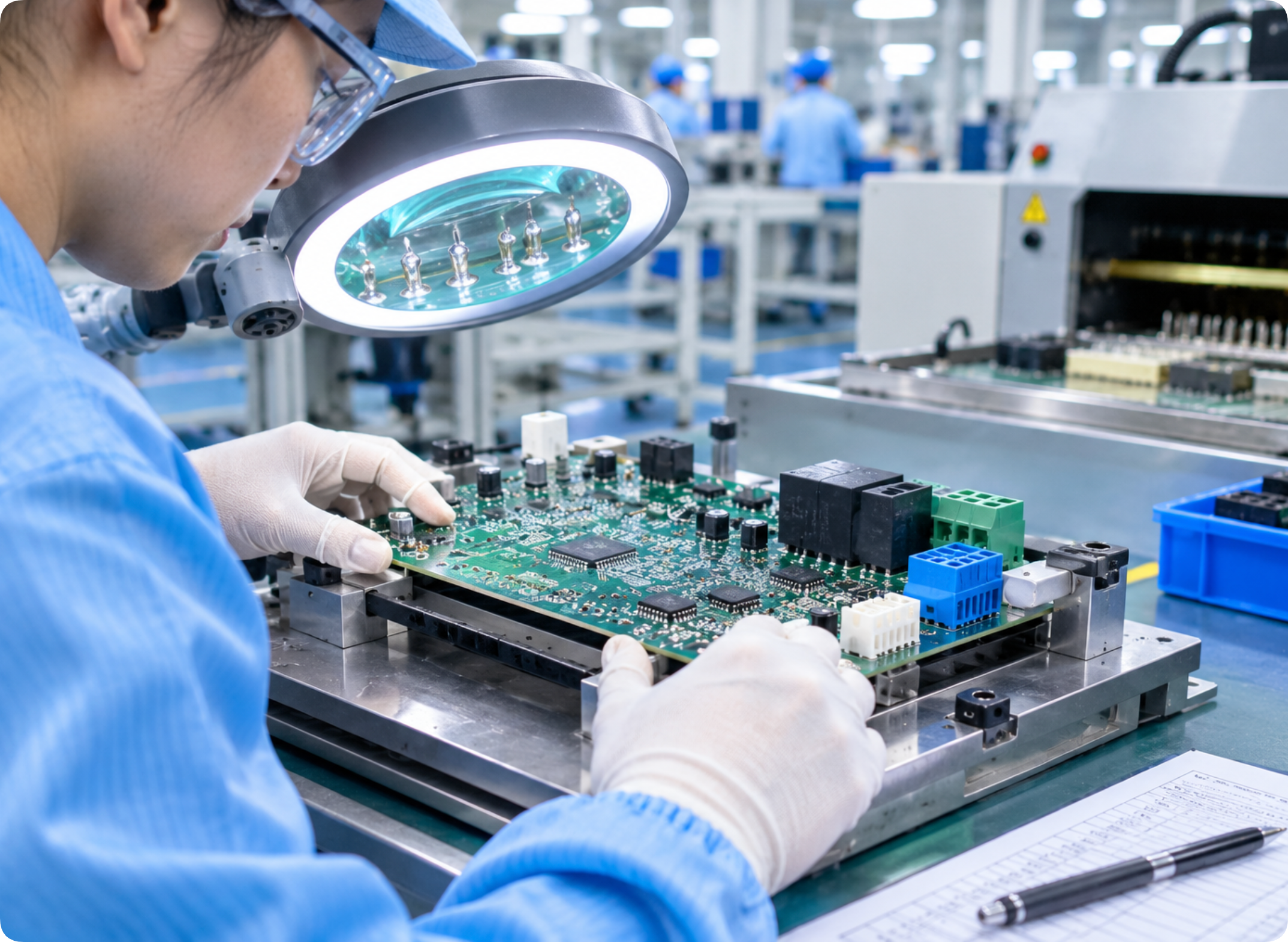
Industry commentators periodically declare traditional through-hole assembly obsolete, yet modern manufacturing floors consistently prove them wrong. DIP Assembly remains essential because certain electronic components cannot rely solely on surface-mount technology. High-current power connectors, heavy-duty transformers, mechanical relays, and hardware subjected to rigorous physical stress require robust component leads inserted through the printed circuit board and soldered securely on the reverse side.
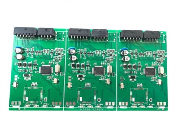
This technological evolution is quieter than surface-mount advances but equally vital. Advanced selective soldering has replaced traditional wave soldering for mixed-technology circuit boards, fixture automation has improved, and sophisticated automated optical inspection (AOI) reads solder joints accurately. Crucially, DIP assembly now seamlessly shares production lines with high-density SMT processes without causing bottlenecks. A mixed assembly board featuring 90% surface-mount components and 10% through-hole parts no longer requires multiple disparate suppliers and costly freight logistics between facilities.
Automotive-Grade PCBA: Every Year the Bar Moves
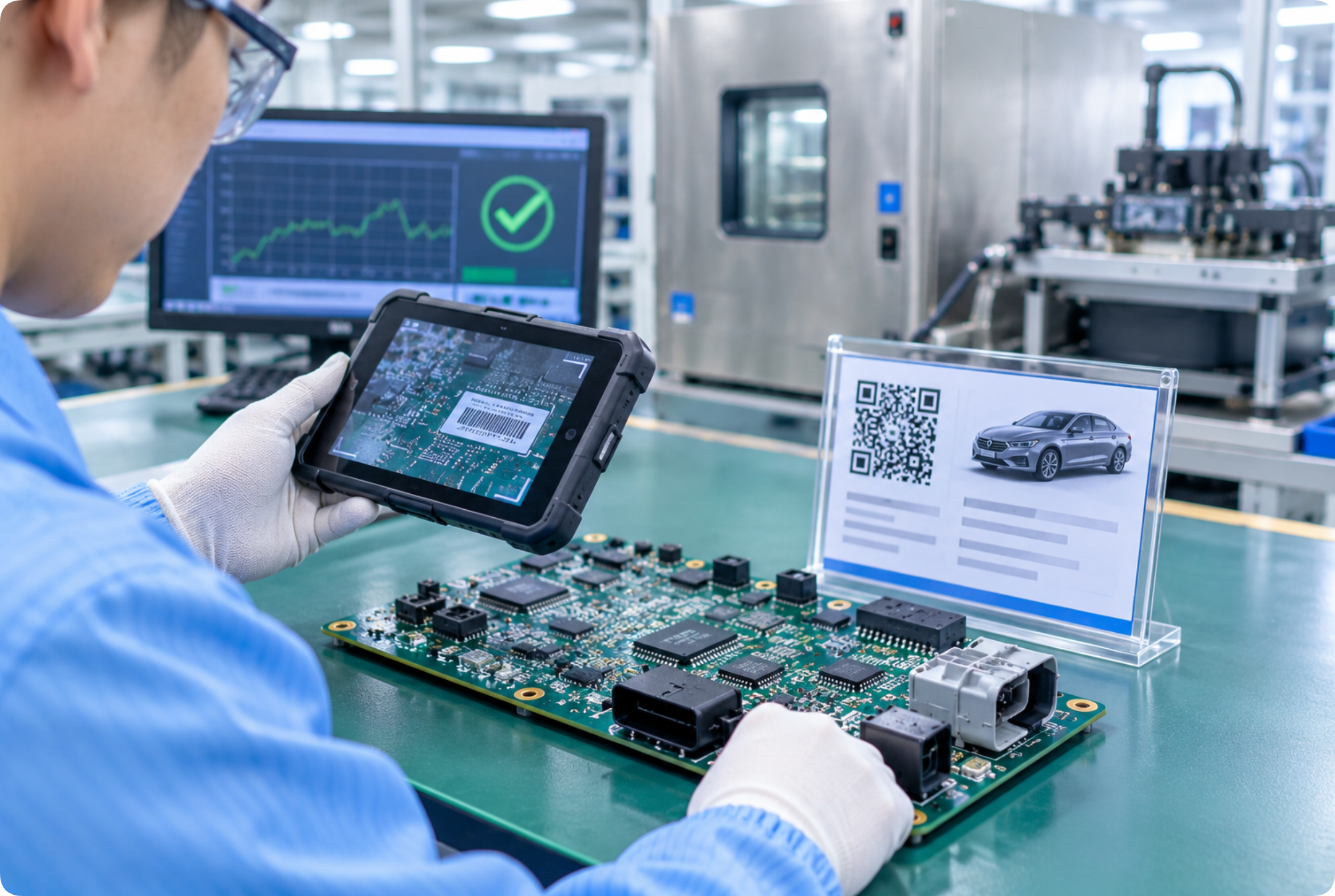
If any manufacturing track has elevated its quality benchmarks drastically, it is automotive electronics. Circuit boards that passed incoming quality control inspections five years ago would routinely fail modern standards. Custom Automotive Electronics now operate under strict AEC-Q100 reliability principles even when formal certification isn't explicitly mandated, due to demanding operating envelopes: severe thermal cycling, constant mechanical vibration, high humidity, and rigorous traceability requirements reaching back to the bare laminate.
This evolution manifests primarily as engineering discipline rather than hardware changes alone. Extended temperature-rated components, integrated conformal coating considerations at the schematic level, and comprehensive documentation trails enabling field failure analysis down to specific material lots are standard practice. Quality standards advance every model year, and top-tier manufacturing partners treat automotive compliance as an overarching process philosophy rather than a one-time certification checkbox.
A Side-by-Side Scorecard of the Three Capabilities
Evaluating these three manufacturing tracks side by side highlights a clear industry trend: each capability has evolved toward tighter operational integration rather than isolated specialization.
| Dimension | Shell Mold | DIP Assembly | Automotive PCBA |
|---|---|---|---|
| Primary evolution driver | Tooling speed | Shared-line compatibility | Reliability envelope |
| Lead-time trend | Days instead of weeks | One line with SMT | Lot-level traceability |
| Tolerance direction | Finer walls held | Cleaner joints, smarter fixtures | Wider temp and vibration rated |
| Where it still wins | Low and mid volume enclosures | High-stress through-hole parts | Harsh-environment electronics |
| Biggest risk if ignored | Shape frozen too early | Hidden bottleneck on mixed boards | Field failure far from the bench |
Under the Hood: Materials, Tolerances, and Automation
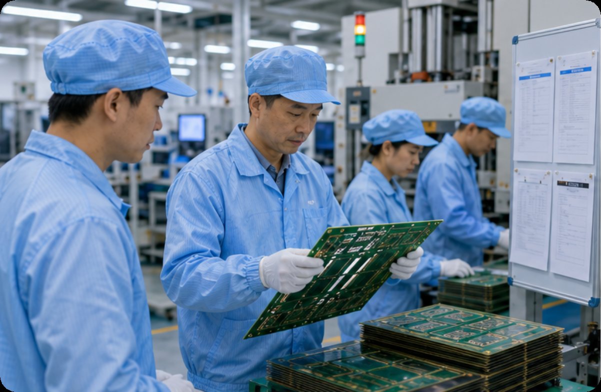
Stripping away marketing terminology reveals a common technological engine driving all three tracks: advanced material science, tighter mechanical tolerances, and extensive automation in quality inspection. Lead-free solder alloys and high glass-transition temperature ($T_g$) laminates empower circuit boards to operate under higher thermal loads and extended lifespans. As component miniaturization pushed packaging down to 0201 footprints and ultra-fine pitches, SMT assembly lines integrated advanced solder paste inspection (SPI) and automated optical inspection (AOI) as mandatory quality gates rather than optional luxuries.
This high level of automation is precisely what allows traditional methods to endure. When every individual solder joint is digitally measured and component placement is fully logged, through-hole assembly ceases to be a manual variable and becomes another verified production step. The true evolution relies less on any single piece of machinery and more on comprehensive digital verification following the product throughout its manufacturing journey.
Where the Three Come Together on One Production Floor
The tangible financial and operational payoff becomes obvious during complex production runs. Consider an industrial automotive sensor module: it requires an enclosure that can be rapidly iterated while firmware development is ongoing, resilient through-hole connectors that surface-mount pads cannot anchor securely, and a circuit board engineered to reliability thresholds far exceeding standard consumer electronics. Distributing these requirements across separate manufacturing facilities introduces multiple logistics loops, inventory queues, and communication gaps regarding mechanical tolerances.
Consolidating production under a single roof through our comprehensive electronics manufacturing services ensures a unified digital data package flows seamlessly from tooling mold to component placement and environmental qualification. Enclosure geometry updates instantly when PCB layouts change, through-hole insertion is fully synchronized on the line, and automotive testing protocols are engineered directly into initial schematic reviews. Technological convergence is the ultimate upgrade; individual manufacturing processes are simply collaborative components.
Scenarios Where the Older Process Is Still the Right Call
Industrial evolution does not mean discarding proven methods entirely. Clear operational scenarios exist where traditional techniques remain optimal. Select shell mold enclosures over expensive hard injection tooling when production volumes remain under a few thousand units or when mechanical geometry is still evolving. Retain DIP assembly whenever interface connectors carry substantial electrical current or withstand physical insertion force that standard surface pads cannot support. Specify automotive-grade process discipline for non-automotive applications whenever deployed hardware operates in high-heat, high-vibration, or inaccessible remote environments.
Engineering expertise lies in recognizing which manufacturing track best suits the specific hardware in front of you, allowing complementary methods to support rather than compete with one another. Applied consistently across a product lifecycle, this strategic judgment transforms manufacturing execution from a series of crisis management loops into a streamlined, predictable success.
Frequently Asked Questions
1. Is shell mold still worth it once volumes climb above a few thousand units?
Usually not as a standalone long-term solution. Once production exceeds several thousand units, hardened steel injection tooling provides superior per-part cost efficiency. However, many successful programs maintain shell mold tooling for spare parts inventory, regional market variants, and early product launches because tooling turnaround times are measured in days rather than months.
2. Does DIP assembly still make sense next to a full SMT line?
Yes, particularly for hybrid mixed-technology circuit boards. Advanced selective soldering allows through-hole sections to coexist alongside dense surface-mount areas within a single production pass, retaining the mechanical retention strength of heavy leads without requiring secondary suppliers or separate production runs.
3. What actually pushed automotive PCBA to its current reliability bar?
The primary driver was the demanding operating environment rather than sheer component density. Extreme thermal fluctuations, continuous mechanical vibration, moisture exposure, and strict regulatory mandates requiring end-to-end traceability of every field failure back to specific build lots forced high-reliability component ratings and rigorous process control into everyday manufacturing practice.
4. How do these three capabilities shorten time to market for a new device?
They effectively eliminate inter-vendor handoffs. When custom enclosures, through-hole assembly, and qualified PCB fabrication reside within a unified digital workflow, design revisions update all dependent processes concurrently rather than triggering delays across multiple external supplier logistics loops, which is where most project schedule slippages occur.
Tags: PCB Manufacturing /
Prev: Supplier Scorecards Are Rewriting Incoming Quality Control for SMT Assembly Buyers
Next: No more...