
PCB Assembly Cost Breakdown: Where Budget Is Really Committed
My view up front: a PCB assembly cost breakdown is not a single number to negotiate down. It is three separate commitments made at three different times, and they do not share the same escape route. One is fixed when a bill of materials is released, one accumulates while boards move down a line, and one is added after the board already works. Teams that treat all three as one figure usually win the first round of pricing and lose the third.
The useful question is not what a board costs, but at which point each part of that figure stops moving. Spend that is still negotiable is leverage. Spend that has already hardened is just history. The three stages below sit in a fixed order, and the order is the whole story.
Three Stages, Three Kinds of Money
A board carries three cost layers, and they behave differently. The first is committed in commercial documents, before any machine runs. The second is charged by measured work, so it scales with volume rather than with intention. The third is applied near the end, once the assembly is electrically sound, and it is the layer most people underestimate because it arrives when the project already feels finished.
What makes the sequence worth studying is asymmetry. A decision made in the first stage can still be revised, at a price. A decision already spent in the second stage can be revisited only by redoing work. A decision applied in the third stage touches a functioning board, which is why it carries consequences the other two do not.
Stage One — The BOM Signature Sets the Floor
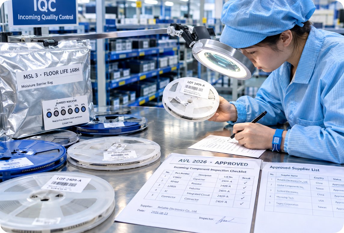
Most product companies now concentrate on design and sales and hand the material side to a partner. Under that model the customer supplies design documents, and the manufacturer buys the parts and completes the assembly against those documents. The saving is not only the difference between two quotations. It is the removal of an internal purchasing, inspection and storage function that would otherwise sit on the books with its own headcount and its own stagnant stock.
What fixes the figure at this stage is a pair of forces: price and continuity of supply. Centralised buying through original manufacturers and authorised agents addresses both, and a long-standing relationship with those channels is what earns priority allocation when a part goes short. The alternative, buying from whichever trader has stock this week, is where quality consistency quietly breaks down. A recognised part number arriving through an unrecognised route is the most expensive kind of saving. This is the stage where electronic component procurement decides the floor that everything downstream rests on, and it is also the stage where a supplier approval file, sample recognition and AQL sampling on core parts turn a promise into a record.
Stage Two — What a Placement Line Charges For
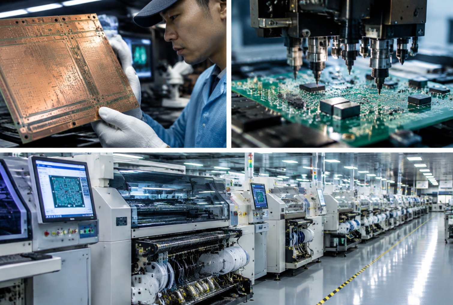
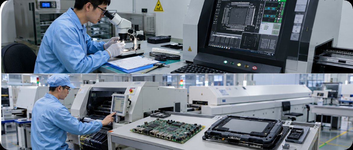
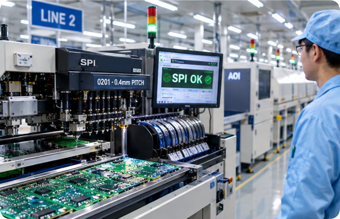
The second layer is measured work, which is why it is the easiest to forecast and the easiest to misjudge. Capacity comes first: four fully automatic high-speed placement lines with automatic board loaders, automatic solder paste printers, solder paste thickness inspection, multi-zone reflow, optical inspection and X-ray on the same floor. That equipment set is what allows 0201 components and 0.4 mm pitch BGA and QFN packages to be routine rather than heroic, because paste volume and placement accuracy are checked before the board reaches reflow instead of after. Quality systems behind it include ISO 9001:2015 and ISO 13485 for medical devices, plus IATF 16949 for automotive electronics.
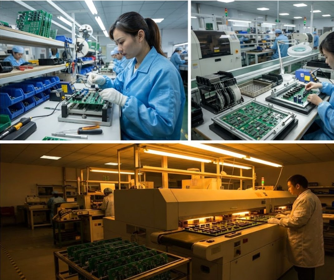
When the price is quoted per joint, the work becomes countable. The rate itself is not published as a number; it comes out of your own BOM and Gerber files, and what it tracks is joint count and board quantity rather than the value of the parts. Hand soldering and the one-time fixtures that wave soldering needs sit outside that quote, which is why a small prototype and a production run can look wildly different per unit. At volume, a team of twenty in quality covering incoming, in-process and outgoing inspection plus ten engineers running design-for-manufacturability review is what keeps SMT assembly predictable, and a normal three to five working day lead time is the visible edge of that discipline.
Stage Three — The Last Step You Can Still Undo
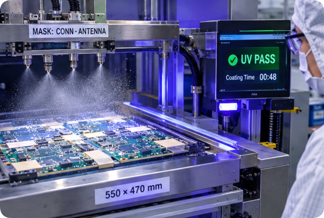
The third layer is added after the board functions, and that timing is exactly what makes it different. A dedicated spraying line with two units, ultraviolet inspection and baking in one continuous flow applies a transparent film whose job is insulation, moisture resistance, leakage resistance, impact and dust protection, corrosion resistance and ageing resistance. Manual brushing cannot hold that consistency; the familiar failure modes are uneven thickness, contamination in the coating and material creeping into places it must never enter, such as display windows and sockets.
Because the process runs late, it has to be selective. Connectors, antennas, Wi-Fi modules and heat sinks are masked so they stay coated-free, boards up to 550 mm by 470 mm can be handled on purpose-built carriers, and fan-shaped spraying combined with needle spraying covers dense, tall-component areas that a single nozzle would miss. Double-sided spraying and baking are supported, and an average of 0.5 to 3 minutes per board keeps throughput real rather than theoretical. This is where PCBA Three-Proofing Paint earns its place in the model, and it is the layer that turns a working board into one that stays working in a humid cabinet or a coastal installation.
Freedom to Change, Stage by Stage
The table below compares the three layers by how much room each one leaves once the figure is set. It is deliberately qualitative, because the published numbers describe rates and timings rather than the price of undoing a decision.
| Layer | Fixed when | What sets the figure | Cost of revising later |
|---|---|---|---|
| Electronic component procurement | At bill of materials release | Part selection, source channel, order quantity | Substitute approval, fresh sample recognition, schedule slip |
| SMT assembly | At first article approval | Joint count, board quantity, stencil and fixture spend | New program, new stencil, process re-qualification |
| PCBA three-proofing paint | After the coating pass | Board size, masking effort, cure cycle | Chemical strip, re-clean, re-spray, possible component damage |
What Each Service Publishes
Rather than estimate, the table below repeats only what the service pages state outright. Where a page does not publish something, it is left out instead of filled in. A model built on published figures can be defended line by line later.
| Service | Published figure | Conditions stated on the page |
|---|---|---|
| Electronic component procurement | Ten-year supplier relationships | Centralised buying with original manufacturers and authorised agents; AQL sampling on core components |
| SMT assembly | No list price; quotation follows your own BOM and GERBER documents | Special process requirements such as manual welding, and one-time wave soldering fixtures, priced separately and not included |
| SMT assembly | Three to five working days | Applies when materials are on hand; excludes public holidays |
| PCBA three-proofing paint | 0.5 to 3 minutes per board on average | One dedicated line with two spray units, ultraviolet inspection and baking |
| PCBA three-proofing paint | Boards up to 550 mm by 470 mm | Selective masking of connectors, antennas, Wi-Fi modules and heat sinks |
Why Late Edits Multiply
Teams that have run a few programmes notice a pattern: the same change costs more depending on when it lands. Swap a part before the bill of materials is released and the paperwork is administrative. Swap it once the assembly is built and the change walks through a loop that includes re-qualification, so engineering time reappears in the schedule rather than the invoice.
Through-hole work makes the pattern concrete. A per-joint rate for wave soldering looks lower than hand soldering on paper, but that rate assumes a fixture exists. Build the fixture for a design that is still moving and the fixture is scrap by the second revision. This is why DIP assembly is best costed after the hole pattern is frozen, not before. The same logic runs in the other direction at the end of the line: once the coating has cured, correcting an assembly means stripping the film, cleaning, re-masking and spraying again, and every one of those steps touches a board that was already good.
Questions to Settle Before Releasing Tooling
Four questions do most of the work. First, which parts are single-sourced, and what has been recognised as a substitute before the shortage arrives. Second, how many joints the design actually carries, because that number moves the second layer far more than any conversation about part price. Third, which areas must stay uncoated, since masking decisions taken late add labour to a step that is already near the end. Fourth, what the review after first article is allowed to change.
None of these require a spreadsheet. They require deciding the sequence in advance and then holding it, because the order in which the three layers harden is also the order in which your leverage disappears. A partner that publishes its rates, its lead times and its process limits, and that runs our electronics manufacturing services under one quality system from incoming inspection through final packaging, is easier to hold to a model than one that answers each question with a promise. If you want to see how the three layers line up for a specific design, send the bill of materials and drawings and ask for the breakdown in writing. Teams that want more background before that conversation can learn more about our manufacturing capabilities, and start the model from there.
Tags: PCB assembly cost breakdown / SMT assembly cost / PCBA three-proofing /
Prev: PCB Fabrication, Aging Test and EMS Electronic Manufacturing: Where Compliance Is Really Decided
Next: No more...