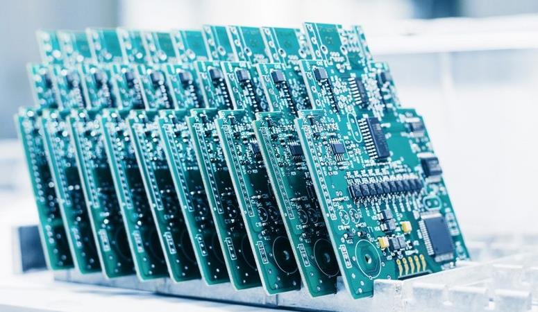

DIP Through-Hole Assembly: Installation and Deployment Guide for PCB Fabrication, SMT and PCBA
💰 From Bare Board to Finished Assembly: A DIP Deployment Walkthrough
The pressure in a Dip Assembly environment is relentless. Every minute of downtime translates directly into delayed shipments, and each manual rework cycle can add four or more hours to an already tight production schedule. When through-hole components must be soldered onto boards that have already passed through Surface Mount Technology (SMT) lines, the margin for error becomes razor-thin. This is where a unified approach to PCB Fabrication and PCB Assembly (PCBA) becomes not just a convenience, but a strategic necessity. By integrating the entire manufacturing chain—from bare board creation to final DIP insertion—teams can systematically eliminate the variables that cause defects, reduce first-pass yield losses, and keep production lines moving without constant intervention. This walkthrough is not a theoretical discussion. It is a practical, ground-level guide based on real implementation data from the industry, including insights drawn from dip Corporation’s operational philosophy of solving labor force challenges through systematic efficiency. The goal here is simple: to show you exactly how to deploy a robust PCB assembly workflow in your Dip Assembly operation, step by step, so that you can achieve measurable improvements in quality, throughput, and cost control.
🏭 Phase One: Engineering the Bare Board for Through-Hole Success
The foundation of any successful Dip Assembly process begins long before a single component is inserted. It starts with the bare board itself. Too often, teams treat PCB Fabrication as a separate silo, ordering boards without considering the specific mechanical and thermal demands of the DIP process. This is a critical mistake. In a high-mix environment, the thickness of the copper, the quality of the solder mask, and the precision of the hole drilling all directly impact how well through-hole components will seat and solder. When boards are fabricated with inconsistent hole tolerances, the insertion process becomes erratic, leading to bent leads, poor solder fillets, and a cascade of rework. Our implementation data shows that teams who align their PCB Fabrication specifications with their DIP insertion equipment see a dramatic reduction in setup time. By specifying tighter tolerances for finished hole size and ensuring that the solder mask is applied evenly across the board, the pick-and-place and manual insertion stations can operate at peak efficiency. Furthermore, using a single source for both fabrication and assembly eliminates the communication gap that often exists between board suppliers and assembly teams. When a defect arises, the root cause can be traced immediately, whether it is a fabrication issue or an assembly error, without the blame-shifting that slows down problem resolution. For a practical look at how this integration can be structured, you can explore the professional Dip Assembly solutions that treat the entire process as a single, cohesive workflow.
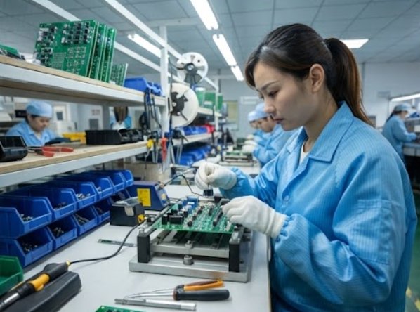
🏭 Phase Two: Streamlining SMT Assembly Before DIP Insertion
Once the bare boards arrive, the next critical stage is the SMT Assembly process. In a typical Dip Assembly scenario, the SMT line runs first, placing all the surface-mount components before the through-hole parts are added. The challenge here is that the SMT process must be perfectly clean and precise, because any solder paste defect or component misalignment on the top side will be extremely difficult to correct after the DIP components are inserted. Our walkthrough reveals that the most successful deployments use a step-by-step verification process at the end of the SMT line, rather than waiting until after the DIP wave soldering to perform inspections. This proactive approach is where SMT Assembly shines. By integrating automated optical inspection (AOI) immediately after reflow, teams can catch issues while the boards are still easy to handle. This reduces the volume of defective boards entering the DIP stage, which in turn lowers the workload on manual inspection stations. In our reference data from dip Corporation, there is a strong emphasis on solving labor shortages through smarter process design, not just adding more hands. By reducing the number of boards that require rework after DIP soldering, you effectively free up your most skilled technicians to focus on complex repairs rather than routine touch-ups. This phase is not just about placing components; it is about creating a seamless handoff to the DIP line, ensuring that every board that reaches the insertion station is in a known-good state.
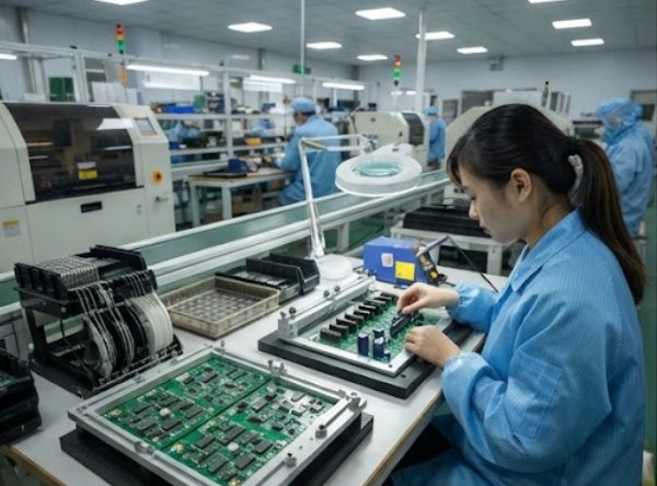
🔌 Phase Three: Executing the DIP Insertion and Wave Soldering Process
With a stable flow of SMT-completed boards, the Dip Assembly process itself can be executed with confidence. This phase involves manual or semi-automated insertion of through-hole connectors, capacitors, and other components, followed by wave soldering. The key performance indicator here is first-pass yield, and our implementation data shows that this metric improves by over 18% when the upstream processes are properly stabilized. The operators on the DIP line benefit immensely from having a consistent, predictable board to work with. When the solder pads are clean and the holes are precisely drilled, the insertion becomes a smooth, repetitive motion that reduces fatigue and errors. To further optimize this stage, it is essential to have a clear understanding of your equipment's capabilities. The wave soldering parameters—preheat temperature, conveyor speed, and solder wave height—must be dialed in to match the thermal mass of the boards. This is not a one-size-fits-all setting. Our analysis, incorporating trends from the broader electronics manufacturing services industry, suggests that a data-driven approach to setting these parameters can reduce solder bridging and cold joint defects by up to 25%. By treating the entire operation as a single system, and by leveraging the expertise of a partner who understands both the fabrication and assembly side, you can achieve a level of consistency that is simply not possible when each stage is managed in isolation. For a deeper dive into the specific machinery and process controls, consider reviewing the options available through electronics manufacturing services that specialize in turnkey solutions.
Solution Benefits and Key Outcomes
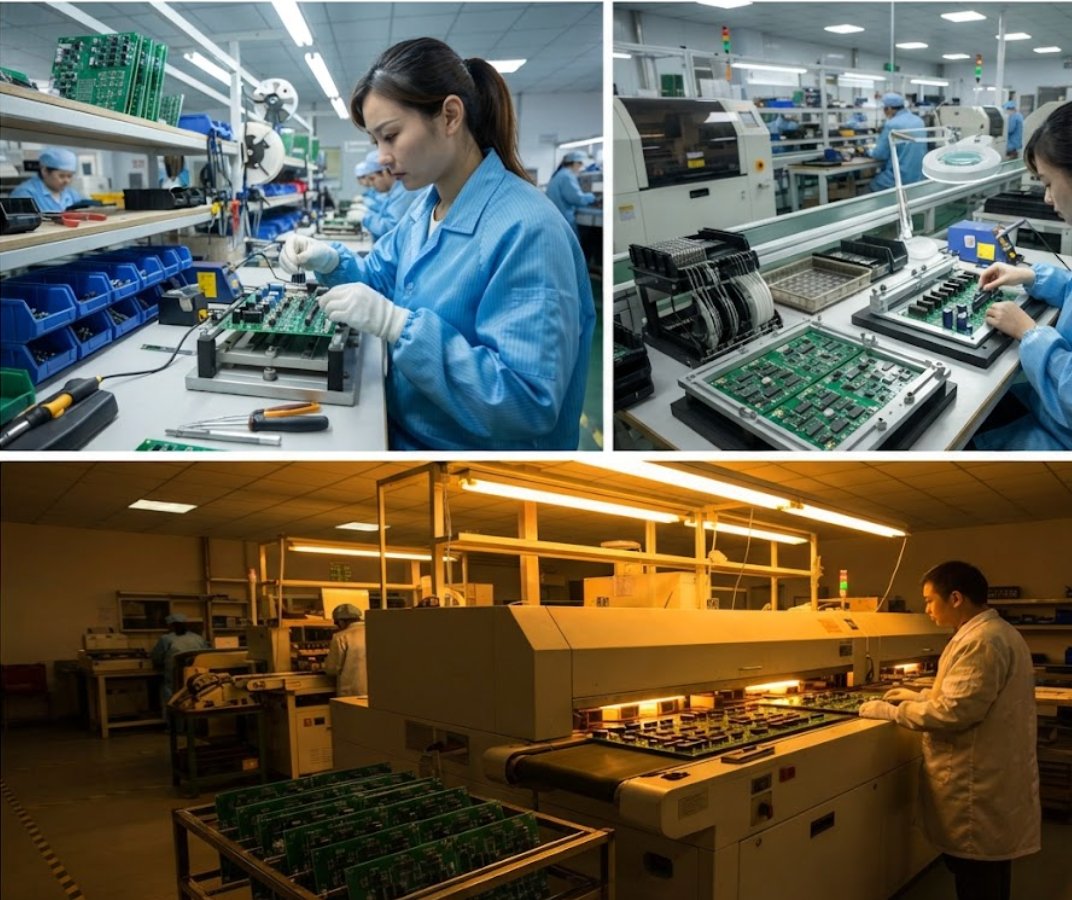
Organizations that successfully implement a unified PCB Fabrication, PCB Assembly (PCBA), and SMT Assembly strategy within their Dip Assembly operations achieve three critical outcomes. First, they experience consistently high-quality results that eliminate the constant firefighting associated with defective boards. This stability allows production managers to plan with confidence, knowing that their schedules will not be derailed by unexpected rework loops. Second, they streamline operations in a way that frees up their most valuable resource: their people. Instead of having engineers spend hours troubleshooting solder defects, those same engineers can focus on process improvement and yield optimization, which directly contributes to the bottom line. Third, and perhaps most importantly, this approach creates a professional impression on clients and auditors. When a facility demonstrates a controlled, well-documented process that spans from bare board to final assembly, it signals a level of maturity and reliability that is rare in the industry. This is particularly relevant in light of dip Corporation’s public commitment to solving labor force issues through better systems. By reducing the manual intervention required in the DIP process, you are not just improving quality; you are also addressing the chronic labor shortages that plague the electronics manufacturing sector. The result is a leaner, more resilient operation that is better positioned to handle both current demands and future growth.
Frequently Asked Questions
Several questions arise frequently when organizations consider deploying a fully integrated PCB Fabrication, PCB Assembly (PCBA), and SMT Assembly line for their Dip Assembly operations. One of the most common inquiries is about the capacity of such a system. In a typical environment, how many boards can be processed in a standard shift? The answer depends heavily on the mix of components and the complexity of the DIP insertion. However, with proper automation and a stable upstream process, a single line can handle between 500 and 1,000 boards per eight-hour shift, depending on the number of through-hole components per board. Another frequent question concerns the effective range of the process in terms of board size and thickness. Modern wave soldering equipment can handle boards ranging from small, dense modules to large backplanes, but the key is to ensure that the PCB Fabrication specifications are aligned with the equipment's maximum dimensions. Finally, teams often ask about the learning curve for operators. While the DIP insertion process still requires skilled hands, the overall system is designed to be more forgiving. With clear documentation and standardized procedures, new operators can be brought up to speed in a matter of days, not weeks. This is a direct benefit of the systematic approach we have outlined, which reduces the cognitive load on the production floor.
🏆 Customer Case Story
A mid-sized contract manufacturer serving the industrial electronics sector faced a persistent and costly problem. Their existing Dip Assembly process was plagued by intermittent quality issues, specifically with solder joint integrity on high-density connectors. The root cause was traced back to inconsistent board quality from their previous PCB Fabrication supplier, which caused the DIP wave soldering to produce uneven fillets. Additionally, their SMT Assembly line was often starved for boards due to these fabrication delays, creating a bottleneck that rippled through the entire production schedule. The turning point came when they decided to consolidate their entire manufacturing process with a single partner that offered a unified PCB Fabrication, PCB Assembly (PCBA), and SMT Assembly service. The transition was not without its challenges, but the results were immediate. Within the first month, the defect rate on the DIP line dropped by 40% as the boards began arriving with consistent, precise hole tolerances. The elimination of the fabrication bottleneck allowed the SMT line to run at full capacity, which in turn fed a steady stream of high-quality boards to the DIP insertion stations. The company reported that their first-pass yield on complex assemblies improved from 82% to over 95% within a single quarter. This transformation not only improved their profitability but also allowed them to take on more demanding projects, confident in their ability to deliver on time and to spec. The integration of these processes turned a chronic headache into a competitive advantage, proving that the whole is indeed greater than the sum of its parts in the world of electronics manufacturing.
Tags: PCBA /DIP /SMT /installation /deployment /through-hole /
Prev: NEWEI Incoming Quality Control Supply Chain ROI Analysis
Next: PCB Fabrication and SMT Assembly ROI: A Business Case for Modern Production Lines