
How PCBA Three-Proofing Paint Cut Field Failures for a Medical Device OEM
Every electronics OEM eventually runs into the same nightmare: a product that performs flawlessly in the lab yet starts failing the moment it reaches the field. For one medical device manufacturer in Shenzhen, that nightmare arrived as a steadily rising return rate on its portable infusion pump. Hospitals sent units back with corrosion spreading across the main board, cracked plastic housings, and intermittent sensor faults that defied reproduction on the bench. By the time it asked for help, the company had already lost two distribution contracts. This article walks through the failure analysis, the three-part redesign, and the measurable results that followed.
If you are responsible for customer case management, you know this challenge all too well: field failures that cut into uptime, inflate warranty costs, and erode user confidence. When the OEM brought its problem to a professional Customer Case review, the engineering team did not rely on guesswork. It tore down every returned unit, logged each failure mode by category, and rebuilt the product around three proven technologies: a conformal coating for the board, a stronger enclosure, and a fully custom board layout.
🏥 1. A Rising Return Rate on the Production Floor
The customer produces portable infusion pumps that hospitals in Southeast Asia and South America use for controlled drug delivery. Over eight months, the field return rate climbed from 1.2 percent to 3.8 percent. With a monthly shipment of roughly 8,000 units, even a small percentage swing means hundreds of failed pumps, and each return carries the cost of expedited replacement, freight, and lost trust with procurement teams.
Every returned unit shared a similar signature. Inspectors found greenish corrosion clustered around the power connector, dulled solder joints on the sensor header, and a white residue running along the PCB edge. Roughly one unit in six also showed a cracked plastic housing near the screw boss, with water ingress marks around the crack. The failures concentrated in humid, coastal climates, pointing to a moisture problem rather than a component-quality problem.
2. Root-Cause Analysis: Moisture, Corrosion and Cracked Housings
The teardown covered 247 returned units, and the findings were remarkably consistent. Corrosive contamination on the bare PCB accounted for 54 percent of the failures, showing up as electrical leakage and open circuits on unprotected traces and solder joints. Mechanical damage to the housing, which let water enter the enclosure through hairline cracks, caused 27 percent of the failures. The remaining 19 percent combined both modes: a housing crack followed by corrosion on the now-exposed board.
The conclusion was unambiguous. The bare boards were unprotected against condensation and airborne salts, and the original enclosure lacked the rigidity to survive drops, shipping vibration, or an over-torqued screw during maintenance. The OEM faced two paths: keep shipping a marginal design and watch the return rate climb, or redesign with protection as the first design goal. The company chose the second path.
🔍 3. The Combined Fix: Coating, Mold and Custom PCBA
3.1 Sealing the Board Against the Environment
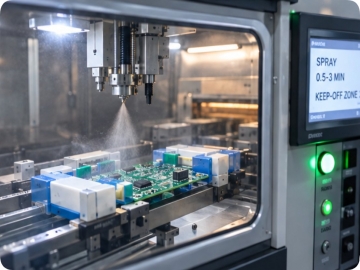
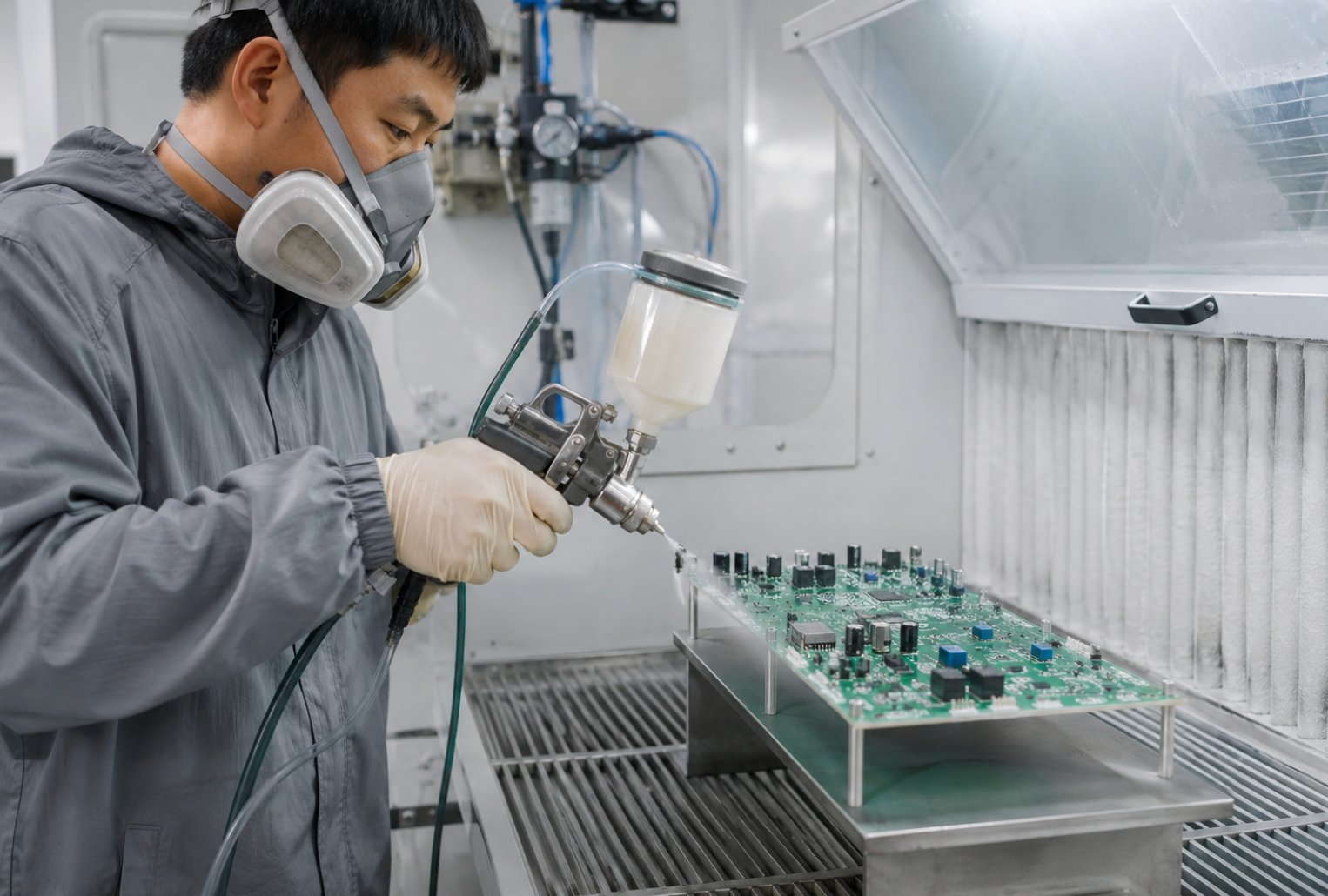
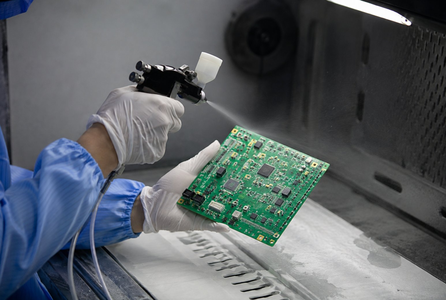
The first change was applied at the board level, and it targeted the largest share of failures. Instead of shipping bare PCBs, the new design routes every board through a PCBA Three-Proofing Paint process that deposits a thin conformal film over the assembled components. The coating forms a continuous barrier against moisture, salt spray, and fungal growth, directly addressing the 54 percent of failures that began as corrosion on unprotected traces and solder joints. It is applied selectively so test points and connectors stay accessible for programming and rework, with a film thickness of 10 to 30 micrometers.
3.2 Shell Mold: Structural Protection for the Enclosure
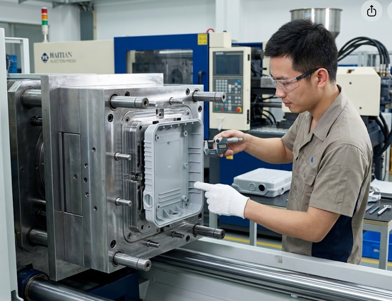
The second change tackled the cracked housings. The OEM replaced its two-piece enclosure with a Shell Mold design that adds reinforced ribbing around the screw bosses, a tongue-and-groove seam on the parting line, and a molded-in rubber gasket channel that lifts the enclosure rating to IP54. Drop tests from 1.2 meters produced no cracks, and the tighter seam eliminated the water ingress that had been killing boards after even minor housing damage.
3.3 Custom Electronic Devices PCBA: Rebuilding the Board for Field Duty
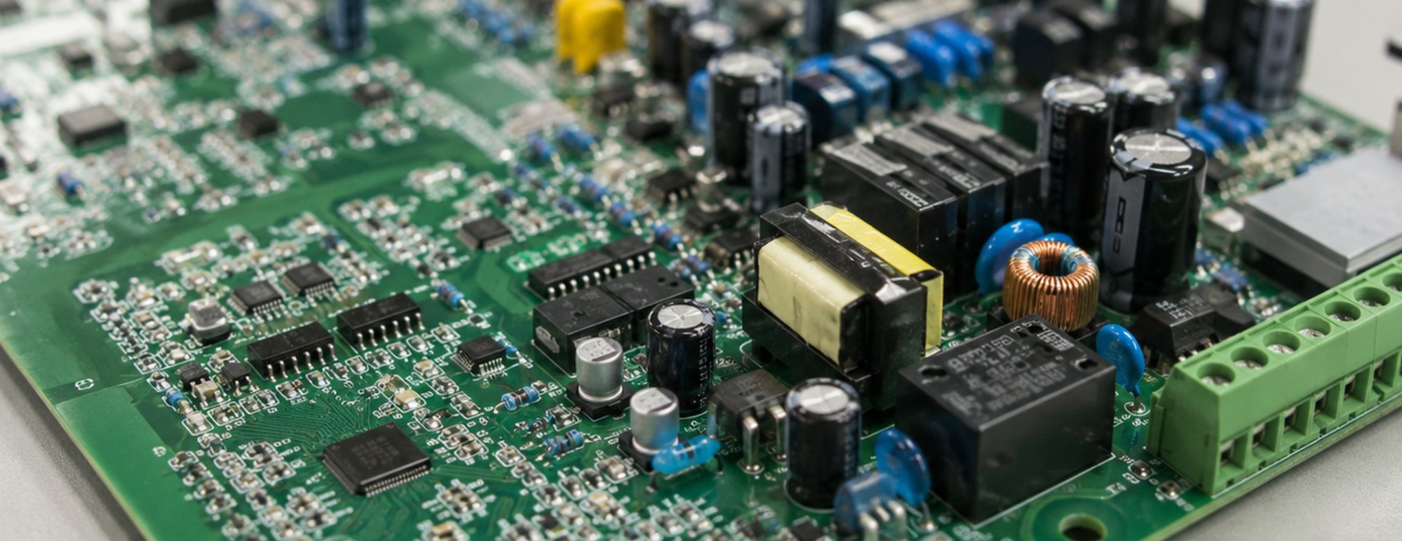
The third change was the most invasive, and it removed the root causes a coating alone could not fix. Instead of patching the old layout, the OEM ordered a complete redesign of the board as a Custom Electronic Devices PCBA. The layout team moved the power connector away from the sensor header, widened the ground plane, added coating keep-outs around test points, and removed two connectors that had been the most common source of cold solder joints in the field. The result was a board engineered for field duty rather than for the production line.
🎯 4. Implementation Guide and Measured Outcomes
The deployment followed a staged plan that gave the team clear checkpoints at every step. First, the team froze the new bill of materials and validated the coating parameters on 50 sample boards. Second, the mold vendor produced the new enclosure and the team ran a 1,000-cycle drop test alongside a 48-hour salt fog test. Third, the redesigned units went through a 30-day hospital pilot in a humid coastal region before the company committed to mass production.
Twelve months after the redesign, the field return rate had fallen from 3.8 percent to 0.6 percent, a reduction of more than 80 percent in failure-related complaints. Rework handling time dropped by roughly 50 percent, because boards no longer needed manual cleaning and corrosion removal, and the pumps now survive a full working day without the intermittent sensor faults that had plagued the old design. The OEM's distribution partners also stopped asking for penalty clauses, a quiet but telling sign that trust had been restored.
🛡️ 5. Product Comparison: Three Layers of Protection
Each technology covers a different layer of risk, and the table below compares them across the factors that mattered most in this case: what each one does, how much protection it adds, and what it costs in lead time and weight.
| Feature | PCBA Three-Proofing Paint | Shell Mold | Custom Electronic Devices PCBA |
|---|---|---|---|
| Primary Function | Conformal coating that seals the board against moisture, salt spray and fungal growth | Precision-molded housing that protects the assembled device from impact and ingress | Fully custom board design, layout and fabrication tuned for the target application |
| Protection Level | Three-proof coverage over traces and solder joints, 10-30 um film | IP54 sealing with reinforced ribs and gasket channel | Design rules for thermal, vibration and EMC performance |
| Impact on Reliability | Eliminates corrosion-driven leakage and open circuits | Prevents housing cracks and water ingress | Removes weak components and poor layout at the source |
| Typical Lead Time | Applied within the standard PCBA production flow | Adds 2-3 weeks for mold tooling | 10-15 days for prototypes, then production batches |
| Weight Impact | Negligible film weight | Adds 30-80 g depending on material | Determined by component count and stack-up |
6. Frequently Asked Questions
Will the conformal coating interfere with repairs? No. It is applied selectively with keep-outs around test points and programming pads, and it can be removed locally with solvent before soldering, so technicians can still perform normal rework.
Can we keep our existing enclosure and just add the coating? Partially, but this case shows the risk of doing so. Corrosion caused only 54 percent of the failures; the rest involved housing damage that a coating cannot prevent. Adding Shell Mold protection covers the mechanical half of the equation, so we recommend applying both layers together.
How long does the redesign take? For a medium-complexity board, the Custom Electronic Devices PCBA redesign adds about two weeks, and mold tooling adds two to three weeks on top of that. Most customers plan for six to eight weeks from design freeze to pilot production.
7. Conclusion and Recommendations
This case shows what happens when a board is protected at every layer. The coating stopped corrosion, the new enclosure stopped physical damage, and the board redesign removed the weak points that generated failures in the first place. Together, the three changes took the return rate from 3.8 percent to 0.6 percent and restored the OEM's standing with its hospital customers and its distributors.
If your product ships with an unprotected board and a thin-walled enclosure, do not wait for the return rate to climb. Talk to an electronics manufacturing services partner about applying the same three-layer approach, and verify the coating and mold options against your own duty cycle and shipping environment before you freeze the design.
Tags: customer case / PCBA three-proofing paint / shell mold / field failure /
Next: Common SMT and DIP Assembly Defects and How to Troubleshoot Them