
PCB Fabrication, PCB Assembly (PCBA) and SMT Assembly: The Technology Evolution Behind Customer Case Success
PCB Fabrication, PCB Assembly (PCBA) and SMT Assembly: The Technology Evolution Behind Customer Case Success
Most engineering teams have lived through the same scenario. The product concept is sound, the market timing is right, and yet the project stalls because the electronics inside were treated as an afterthought. Boards that once carried a few dozen hand-soldered components now stack twenty layers with micron-level traces, and the gap between a promising prototype and a shippable product has never been wider. That is why more organizations are turning to PCB Fabrication, SMT Assembly and PCB Assembly (PCBA) for a fundamentally different approach to building hardware. Understanding this evolution matters, because the capabilities you choose at the board level ripple through every later stage of your project. It is exactly where a professional Customer Case partner can make the difference between a painful rollout and a smooth one.
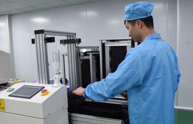
🔌 PCB Fabrication: From Simple Layers to High-Density Interconnect
PCB fabrication is the process that creates the physical board itself, and it has quietly undergone one of the most dramatic transformations in modern manufacturing. Twenty years ago, a typical industrial board carried four to six layers with trace widths around 8 mils, and designers planned around those generous tolerances. Today, high-density interconnect (HDI) boards stack eight, twelve or even more layers while shrinking traces to below 4 mils, and the old rulebook no longer applies. Laser drilling, sequential lamination, blind and buried vias, and impedance-controlled etching have turned fabrication from a routine shop operation into a precision science that supports smaller, faster and more reliable products.
For customer case deployments, the benefits of this evolution are tangible rather than theoretical. Denser boards mean smaller housings, which lower material costs, improve portability and open up industrial designs that would have been impossible to package a decade ago. Better impedance control translates directly into cleaner signal integrity, a requirement that matters for any data-driven product carrying high-speed buses or sensitive analog circuits. Modern fabrication also shortens the journey from prototype to production, because the same tooling and design rules carry through the entire build. Add disciplined testing at the bare-board stage, and most of the surprises that used to surface during final assembly simply disappear.
🏭 Where Components Meet the Board
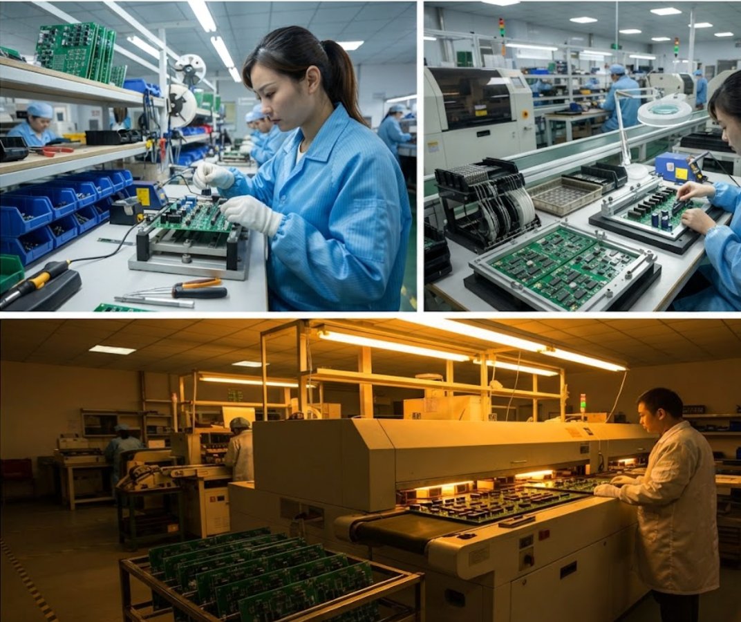
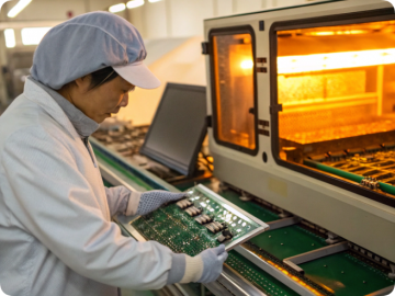
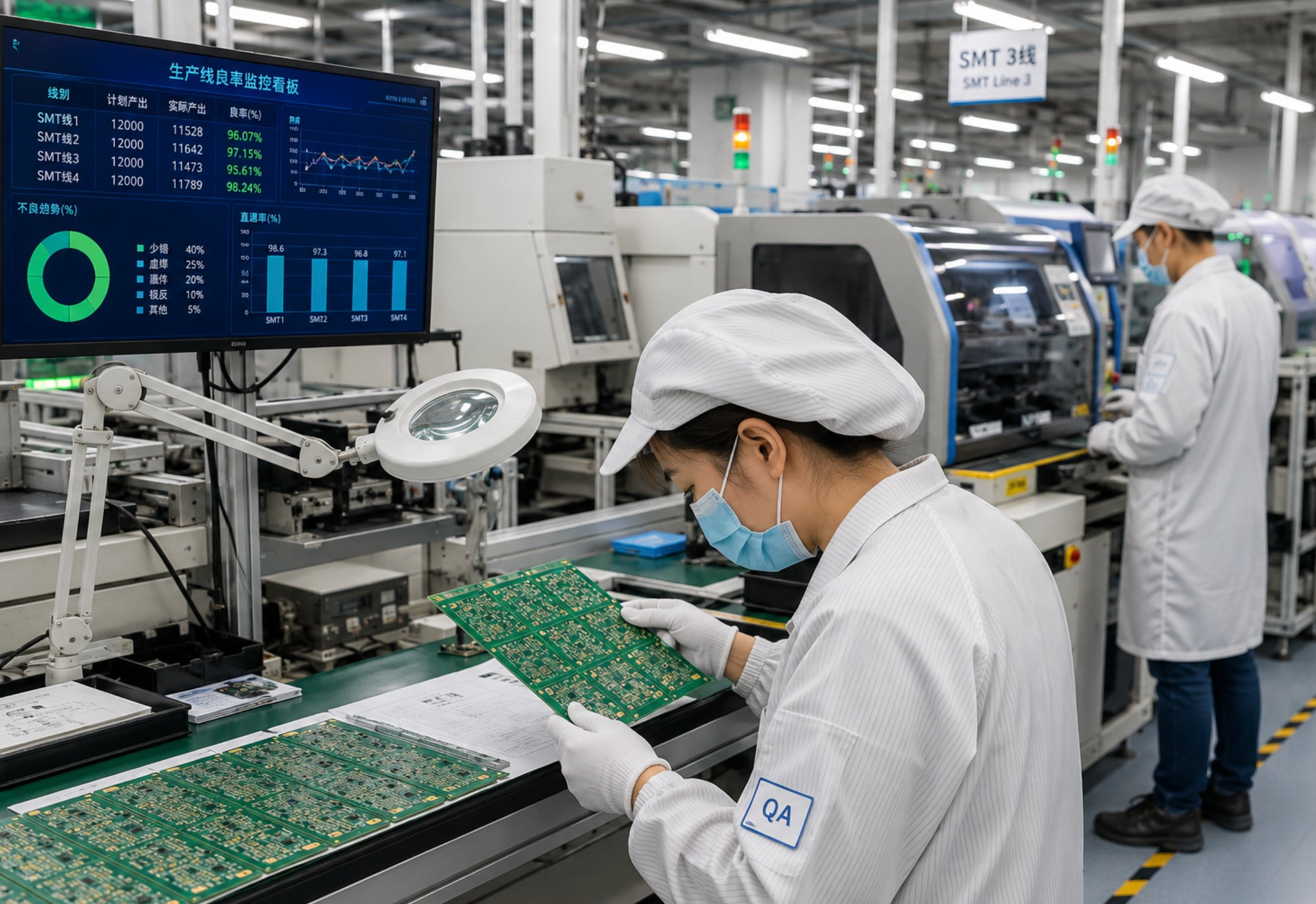
PCB assembly, often shortened to PCBA, is the stage where bare boards become functional products, and it is where the craftsmanship of the past meets the engineering discipline of today. The evolution here has been driven by component miniaturization and by the relentless demand for repeatable, defect-free soldering. In the past, assembly relied heavily on skilled operators placing parts by hand, a method that was slow and difficult to scale. Modern PCBA lines combine precisely machined solder paste stencils, automated placement and carefully profiled reflow ovens to produce consistent joints at high speed. The result is a dramatic reduction in manual error and a corresponding jump in first-pass yield, with fewer boards reworked or scrapped.
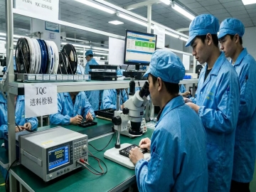
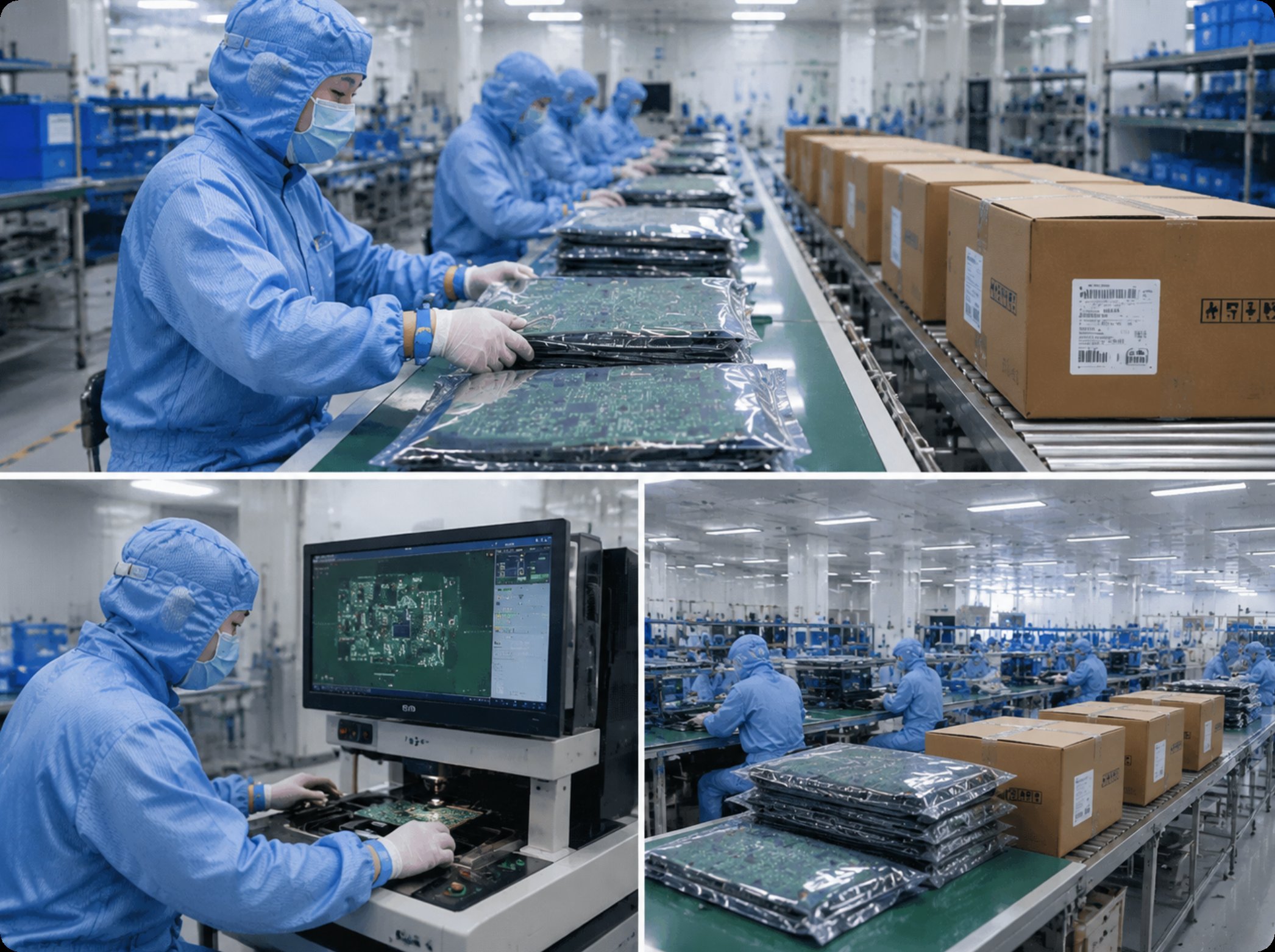
In a customer case setting, the quality of the PCBA stage decides how much time the engineering team spends on debugging later. Boards assembled under controlled processes tend to behave predictably across the whole production batch, which simplifies testing, accelerates commissioning and reduces field failures. Process control extends well beyond the reflow oven: solder paste inspection, automated optical checks, in-circuit testing and functional test fixtures all contribute to a documented quality record. That predictability is why professional installations now insist on disciplined, documented assembly lines rather than workshops that improvise from batch to batch.
🏭 SMT Assembly: Miniaturization and Precision at Scale
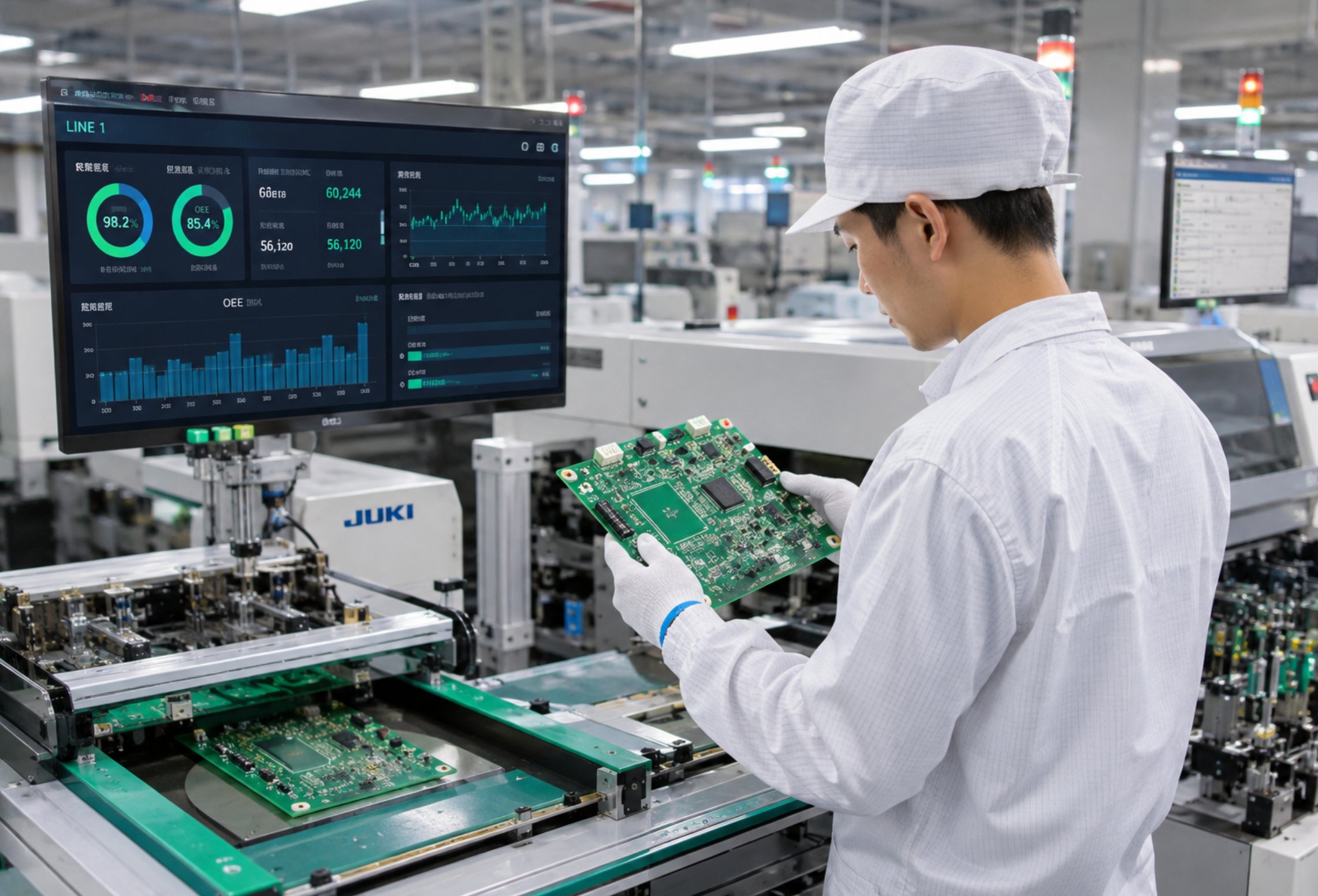
Surface-mount technology, better known as SMT, is the placement technique that makes modern PCB assembly possible. Where through-hole components once required drilled holes and hand-soldered leads, SMT components are placed directly onto the surface of the board and fixed with reflow soldering. This single shift unlocked the miniaturization that powers smartphones, wearable devices and compact industrial electronics. As components shrink from 0603 to 0402 and even 0201 sizes, the placement machines that feed SMT Assembly lines must grow more precise, with high-speed heads and vision systems that align every part within microns. The result is a production floor that can place thousands of components per hour while holding tolerances a skilled operator could never match by hand.
The evolution of inspection has kept pace with placement. Early production lines relied on manual optical checks and spot sampling, which caught only the most obvious defects. Modern lines use automated optical inspection (AOI) systems that catch solder bridges, missing parts and misalignments before boards move to the next stage, and X-ray inspection extends that coverage to hidden joints such as those beneath ball-grid arrays. For customer case projects, this layered inspection translates into fewer returns, shorter commissioning time and a lower total cost of ownership across the product lifecycle.
🏭 Technical Specification Comparison Across the Three Manufacturing Stages
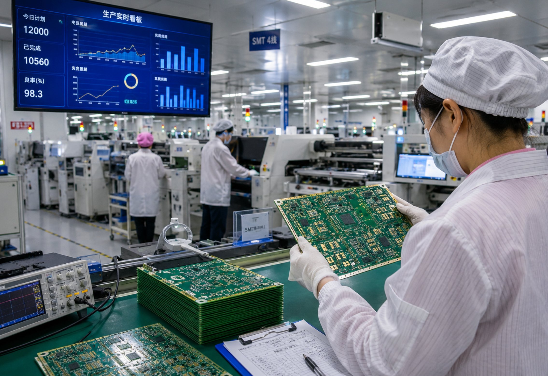
To make the differences concrete, here is a side-by-side comparison of PCB Fabrication, PCB Assembly (PCBA) and SMT Assembly, focused on the specifications that matter most for customer case projects: process depth, component scale, quality control and typical lead time. Each stage excels in a different area, and understanding these differences helps you match the right manufacturing approach to your product's volume, complexity and reliability requirements.
| Capability | PCB Fabrication | PCB Assembly (PCBA) | SMT Assembly |
|---|---|---|---|
| Core Process | Layer stacking, etching and plating of the bare board | Placement and soldering of components onto the board | High-speed automated placement of surface-mount parts |
| Typical Board Complexity | Up to 20 layers with HDI and blind or buried vias | Mixed through-hole and surface-mount layouts | High-density designs with 0201 or smaller parts |
| Component Size | Not applicable, board features only | Standard and fine-pitch components | Ultra-fine-pitch and micro-miniature components |
| Quality Control | Impedance testing and electrical testing of the bare board | AOI plus functional testing of assembled boards | Inline AOI and X-ray inspection for hidden joints |
| Typical Lead Time | Fastest of the three stages | Moderate, depends on component availability | Short when components are in stock |
| Best Suited For | New product development and prototype validation | Low to medium volume finished board production | High-volume repeatable production runs |
🏆 Market Data and Industry Trends in Customer Case Environments
The customer case technology landscape is shifting rapidly, and the data reflects it. Traditional wired systems are being phased out in favor of digital wireless solutions, with early adopters reporting payback periods of under 12 months on equipment that communicates continuously without cabling. Behind that shift sits a quieter revolution in the factory itself. Digitalization is moving through the entire production chain, from digital design hand-off to machine-to-machine data exchange and cloud-based quality traceability. Boards now carry serialized tracking that lets a manufacturer trace every component back to its original lot, turning a quality issue from a mystery into a resolvable data point.
For organizations planning their next project, the practical takeaway is simple: choose a manufacturing partner whose technology has evolved with the industry. Look for modern HDI capability, disciplined SMT placement, AOI-based inspection and the kind of documented quality data that stands up to an audit. These are not luxuries; they are the baseline for delivering boards that perform predictably at volume. If you want to evaluate whether a supplier fits those criteria, you can learn more about our manufacturing capabilities and compare them against your own quality targets before you commit to a production run.
Conclusion
The evolution of PCB fabrication, PCB assembly and SMT assembly has turned electronics manufacturing from a craft into an engineered discipline. HDI structures, micron-level placement, automated inspection and digital traceability now work together to deliver boards that are smaller, faster and more dependable than anything available a generation ago. Teams that embrace these technologies will bring better products to market with fewer surprises and shorter lead times. The future of customer case solutions belongs to those who build on the strongest possible foundation, and that foundation is laid long before the first component is placed on a board.
Tags: PCB technology evolution / PCBA assembly trends / SMT miniaturization /
Prev: PCB Fabrication, PCB Assembly (PCBA) and SMT Assembly: Measured Results from a Customer Case
Next: How PCBA Three-Proofing Paint Cut Field Failures for a Medical Device OEM