
High-Speed SMT Manufacturing, 0201 Micro-Placement & BGA Soldering for Medical Bluetooth Thermometer PCBA
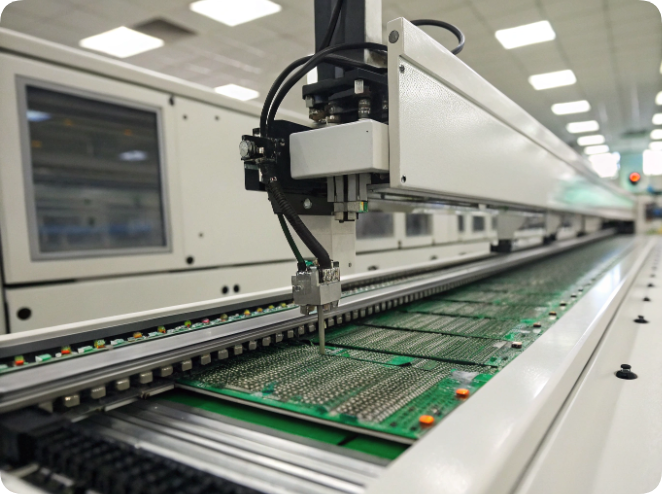
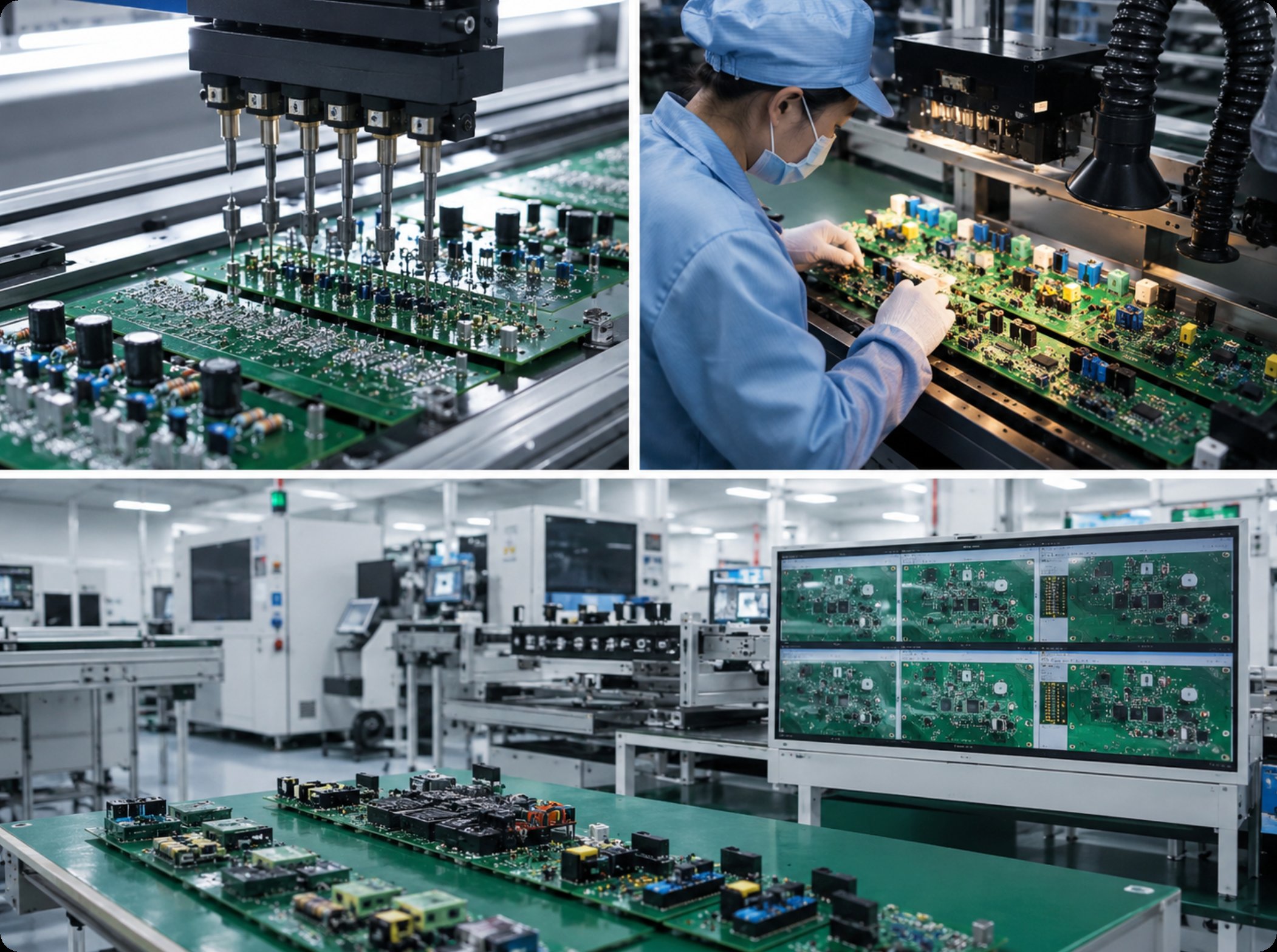
Fig 1 – High‑speed SMT placement line: dual‑beam gantry mounting 0201 passives and Bluetooth ICs for medical thermometer PCBA
Executive Insight: Medical-grade electronic hardware leaves zero margin for manufacturing error. A single microscopic defect—whether a tombstoned 0201 resistor or a micro-void beneath a Bluetooth Low Energy (BLE) System-on-Chip (SoC)—compromises data integrity and puts patient health outcomes at risk. At NEWEI Industrial, our Surface Mount Technology (SMT) production lines bypass standard commercial protocols in favor of aerospace-grade Six Sigma process controls. This technical walkthrough reveals the precise manufacturing mechanics behind our 99.99% first-pass yield for high-density Bluetooth thermometer PCBA engineering, spanning from automated solder paste optimization to advanced vacuum-assisted reflow profile management.
High-Speed SMT Manufacturing, 0201 Micro-Placement & BGA Soldering for Medical Bluetooth Thermometer PCBA
Technical Analysis by NEWEI Industrial Editorial Team · Updated May 2026 · 11 min read
The global remote patient monitoring and smart digital thermometer sector is accelerating toward a projected market valuation of $3.5 billion by 2030. This rapid expansion is heavily propelled by the integration of medical wearables and continuous biosensing technology. Among these innovations, ultra-compact Bluetooth-enabled thermometers require highly dense hardware layouts that are deceptively complex to manufacture.
To fit within modern, ergonomic enclosures often smaller than a standard matchbox, these medical devices depend on high-density Custom PCB Assembly Services. The hardware architecture typically packs ultra-miniature 0201 passive components, fine-pitch Bluetooth Low Energy SoCs (0.4mm pitch Ball Grid Array), high-precision thermistor sensors (QFN packages), and microscopic surface-mount battery terminals into highly confined layout geometries. Consistently maintaining a 99.99% placement yield on these micro-assemblies demands a completely integrated, data-driven manufacturing workflow. This technical guide explores the exact shop-floor protocols executed across our advanced facility.
1. High-Speed SMT Micro-Placement: 0201 Dynamics at 45,000 CPH
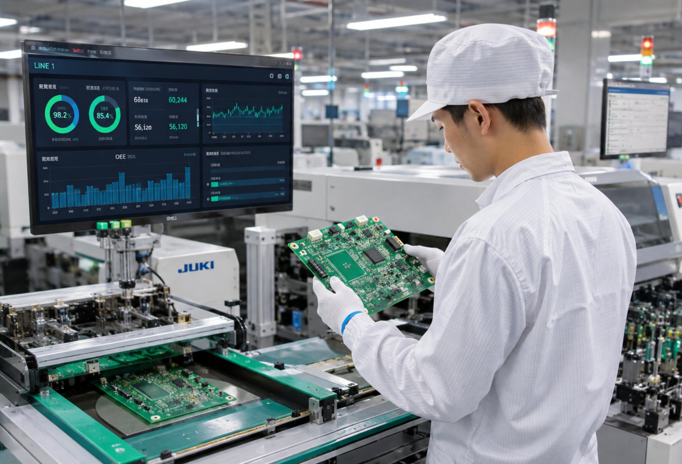
Ultra-miniature 0201 passives (measuring just 0.6mm × 0.3mm) present severe handling challenges during high-velocity assembly. Our medical-grade production floor utilizes an advanced dual-beam, dual-gantry high-speed SMT placement platform capable of sustaining true throughput rates up to 45,000 components per hour (CPH). Precision component verification is governed by real-time, high-resolution side-view vision systems. These cameras analyze every individual component in mid-air during the transfer from feeder to board, immediately identifying and rejecting any part displaying termination anomalies, micro-cracks, or dimensional deviations.
For a standard medical Bluetooth thermometer PCBA, the component bill of materials (BOM) contains between 40 to 60 specialized parts clustered in close proximity. To eliminate the risk of "tombstoning"—the phenomenon where asymmetrical solder surface tension causes a micro-component to stand vertically during reflow—our engineering team reduces standard nozzle placement pressure by exactly 30%. This soft-landing calibration prevents the displacement or squeezing out of the underlying solder paste. Furthermore, automated nozzle-tip maintenance routines execute an intensive solvent purge every 150 pick cycles to eliminate microscopic dust buildup. Through rigorous monitoring via our Manufacturing Execution System (MES) dashboard, our real-world 0201 SMT placement yield maintains a documented baseline of 99.993%.
2. Solder Paste Printing & Closed-Loop 3D SPI Inspection
The foundation of reliable micro-soldering is established long before boards reach the placement machine. For 0201 footprints, even a minor 10% variance in paste deposit volume will lead to catastrophic defects such as bridges or insufficient electrical connections. Our high-precision printing setup features a closed-loop fully automated stencil printer equipped with laser-cut electroformed stencils, utilizing a custom-engineered aspect and area ratio of 0.75 tailored specifically for fine-pitch apertures. Automated under-stencil vacuum solvent cleaning is programmed to trigger after every five print cycles without fail.
Immediately following the paste deposition sequence, 100% of the printed circuit boards are routed directly into an in-line 3D Solder Paste Inspection (SPI) system. Utilizing multi-frequency shadow-free digital fringe projection, the SPI system gauges the precise volume, true area, structural height, and structural X/Y registration offset of every single pad deposit. The system generates a comprehensive, real-time volumetric heatmap. Any circuit pad displaying a volumetric deviation exceeding ±15% is automatically flagged, halting the board from moving downstream to placement. This real-time inspection feedback loop dynamically adjusts the stencil alignment and squeegee pressure of the printer upstream, which has successfully reduced historical paste-related micro-defects by 72%.
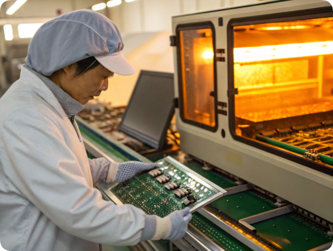
Fig 2 – 3D SPI volumetric heatmap (left) against microscopic post-placement confirmation of 0201 passive networks (right)
3. Vacuum-Assisted Reflow Profiling: Void Elimination in 0.4mm Pitch BGAs
The core intelligence of smart medical thermometers typically relies on a dense 0.4mm fine-pitch BGA or QFN wireless SoC architecture. Standard atmospheric reflow processes often trap outgassing volatile organic compounds, creating internal micro-voids that degrade high-frequency RF signals and fracture under thermal stress. To combat this, NEWEI implements a specialized multi-zone vacuum-assisted reflow oven profile for all medical device assemblies.
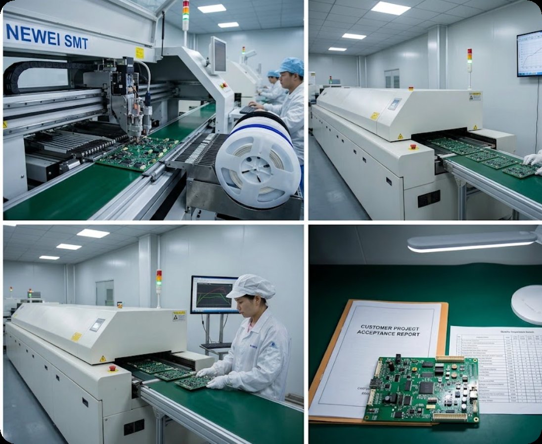
By integrating a highly controlled vacuum extraction stage during the liquidus phase (when the lead-free alloy is fully molten), the ambient pressure is safely brought down to 10 mbar. This pressure differential forces trapped gas bubbles out of the liquid spheres, driving average internal BGA solder void rates down from a standard 18% to under 8%, well below the stringent 20% threshold dictated by medical standards. Our thermal profiling maintains a strict 90-second soak phase between 150°C and 210°C to secure uniform flux activation, peaking cleanly at 245°C for exactly 60 seconds. Post-reflow integrity is validated using high-resolution 3D Automated Optical Inspection (AOI) coupled with regular 3D X-Ray Computed Tomography (AXI) sampling, sustaining a first-pass BGA yield of 99.4%.
4. Advanced DIP & Dual-Wave Soldering for Rugged Through-Hole Interconnects
While SMT micro-components handle processing and communication, through-hole technology (THT) remains indispensable for mechanical interconnects, such as spring-loaded battery contacts, heavy-duty tactile switches, and acoustic buzzers. These components are processed on our dedicated DIP (Dual In-line Package) manual insertion line before entering an automated wave soldering system. Technicians use synchronized ESD-safe workstations where assembly steps are visually cued and completed via barcode confirmation, ensuring complete human-error elimination.
Our automated wave soldering machine employs an advanced dual-wave architecture. The primary turbulent wave delivers high-velocity vertical fluid force to ensure complete solder penetration through tiny plated through-holes (PTH), while the subsequent laminar wave supplies a smooth, stable exit flow to eliminate icicles and solder bridging. Crucial environmental parameters—including a strict pre-heating thermal ramp, targeted spray fluxer atomization, an exact 260°C ±5°C lead-free pot temperature, and precise conveyor speeds—are tracked continually. Operating under an enclosed, high-purity nitrogen ($N_2$) gas blanket reduces dross formation and limits bridging defects by 58%. Assembled modules then undergo a multi-stage ultrasonic aqueous cleaning process with deionized water, followed by a 30-minute forced-convection drying cycle to remove all ionic contaminants.
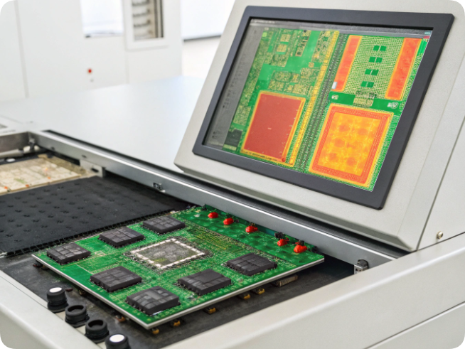
Fig 3 – Manual DIP insertion tracking (left) next to high-purity nitrogen-blanketed selective wave soldering bath (right)
5. Quantifiable Quality Metrics: The SMT Production Dashboard
True manufacturing quality is proven by empirical shop-floor telemetry. Below is the active statistical process control data derived from our continuous digital thermometer manufacturing campaigns:
| Production Process Stage | Key Process Metric Tracked | Achieved Performance Level |
|---|---|---|
| 0201 SMT Component Placement | Placement Accuracy @ 45,000 CPH | ±25µm ($C_{pk} \ge 1.33$) |
| 3D Solder Paste Inspection (SPI) | First-Pass Paste Deposition Yield | 96.8% (3.2% intercepted pre-placement) |
| Post-Reflow 3D AOI | Structural Joint and Orientation Compliance | 97.2% First-Pass Board Yield |
| Vacuum-Assisted BGA Soldering | Average X-Ray Measured Internal Void Area | 8.0% (Medical Spec limit: ≤20%) |
| Dual-Wave THT Soldering | Defective Parts Per Million (DPPM) Baseline | < 520 DPPM |
| Final Functional Testing (FCT) | End-of-Line ICT & Wireless RF Testing Yield | 95.8% Final First-Pass Yield |
6. End-to-End Component Traceability: ISO 13485 Compliance
For medical electronic equipment, raw process capability must always be accompanied by bulletproof traceability. Each individual blank PCB board receives a permanent, unique 2D data-matrix barcode laser-etched directly onto the substrate at the front end of the line. At every single automated and manual station, this unique identifier is scanned by our centralized MES system.
This deep integration enables full component traceability. We log the exact raw material batch number, SMT placement reel lot, solder paste formulation index, operator ID, environmental temperature/humidity values, and the complete, step-by-step 3D SPI and AOI geometric measurement records. In the highly critical field of medical diagnostics, should an end-user device encounter a failure, our quality team can reference the device's cloud record and pull its entire factory floor history within a matter of minutes. This unyielding transparency is central to our stringent quality management system and forms the baseline of our verified ISO 13485 medical manufacturing compliance.
Secure Medical Device Reliability Through Data-Driven PCBA Assembly
The accuracy, operational lifespan, and regulatory clearance of your upcoming medical hardware product depend entirely on manufacturing discipline. Partnering with a specialized electronic manufacturer ensures that your fine-pitch SMT arrays, micro-passives, and sophisticated wireless modules are processed under flawless shop-floor oversight.
Let's Connect – NEWEI Industrial Co., Ltd.
Direct Tel Line: +86-18925218989
Engineering Support: tiger.wang@richitek.com
Official URL: https://www.neweiodm.com
Reach out to our engineering office today to arrange a comprehensive virtual facility audit or upload your full product Bill of Materials (BOM) and Gerber files for a free, thorough Design for Manufacturing (DFM) assessment.
© 2026 NEWEI Industrial. All rights reserved. Professional medical PCBA layout engineering, high-density SMT micro-placement, and specialized electronic OEM/ODM assembly manufacturing solutions.
Tags: Bluetooth thermometer SMT assembly / medical PCBA reflow profiling /