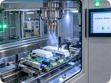

How X‑RAY Full Inspection, ICT/FCT & Traceability Deliver Sub‑150 ppm Defect Rates for Industrial Control PCBA
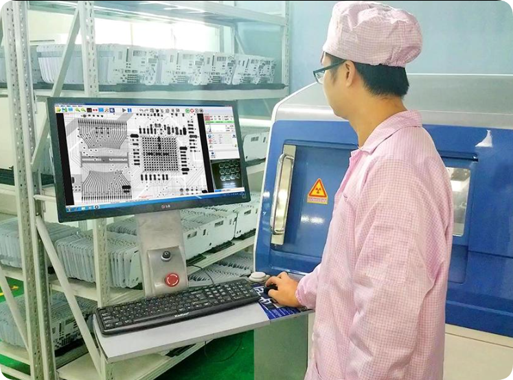
Fig 1 – Automated X‑RAY inspection (AXI) of an industrial control board: real‑time void measurement under a 0.8mm pitch BGA processor
My View: In industrial automation, a single hidden BGA void or an undetected cold solder joint can paralyze an entire production line, triggering downstream financial losses that escalate by tens of thousands of dollars per hour. While automated optical testing excels at surface-level anomalies, advanced X-RAY hardware remains the only definitive methodology to penetrate multi-layer BGAs, QFNs, and massive ground pads. At NEWEI, we implement rigorous 100% automated X-RAY validation for every industrial electronic assembly utilizing bottom-termination components. Combined with in-circuit testing, functional simulation, and component-level traceability, we consistently drive field failure rates below 150 ppm. This breakdown details our comprehensive quality engineering pipeline—from initial first-article sign-off to destructive failure analysis—demonstrating how million-level defect control functions as an active daily discipline on our manufacturing floor.
How X‑RAY Full Inspection, ICT/FCT & Traceability Deliver Sub‑150 ppm Defect Rates for Industrial Control PCBA
By NEWEI Industrial · Updated May 2026 · 12 min read
The global industrial automation infrastructure demands unprecedented electronic hardware survivability. As smart manufacturing systems, IIoT architectures, and edge computing nodes undergo rapid deployments, the underlying hardware must withstand severe environmental stressors, including thermal cycling, mechanical vibration, airborne particulate contamination, and electromagnetic interference. Unlike consumer-grade electronics, a localized hardware failure within a Programmable Logic Controller (PLC), variable frequency drive, or Human-Machine Interface (HMI) immediately halts high-throughput assembly environments, leading to catastrophic operational downtime.
To eliminate these vulnerabilities, manufacturing execution systems must move past basic sampling methods. NEWEI’s specialized production ecosystem addresses these industrial realities through a multi-tiered inspection matrix: 3D inline AOI, 100% automated X-RAY inspection (AXI) for all BGA/QFN packages, high-coverage In-Circuit Testing (ICT), dynamic Functional Testing (FCT), real-time floor patrol QC, automated First Article Inspection (FAI), and comprehensive digital defect traceability. Through this interconnected framework, we maintain an operating defect rate below 150 DPPM across all industrial accounts.
As an industry-certified partner delivering premier Custom PCB Assembly Services, NEWEI embeds these demanding engineering workflows directly into your product’s manufacturing routing. Our global client portfolio spans precision European automation OEMs to advanced robotic developers in the United States, all relying on verified, auditable data packages to secure their critical field deployments.
🔬 1. Inline 3D AOI & 100% Automated X-RAY Inspection: Penetrating Hidden Solder Joints
Immediately following the reflow soldering process, all industrial control boards enter an automated inline 3D AOI system. This phase leverages multi-frequency digital fringe pattern projection to measure true spatial component height, fillet meniscus profiles, and lead coplanarity. This allows the system to identify complex surface defects such as micro-bridging, lifted component leads, tombstoned passive devices, and subtle solder paste alignment shifts. Our custom-trained 3D AOI algorithms, developed across millions of active industrial data points, maintain a false-call metric below 0.7% while intercepting 99.5% of exposed surface anomalies.
However, optical systems cannot evaluate hidden interfaces beneath Ball Grid Arrays (BGAs), Quad-Flat No-Leads (QFNs), or heavy electromagnetic shielding cages. To address this blind spot, NEWEI enforces mandatory 100% automated X-RAY inspection (AXI) for every industrial control board carrying bottom-terminated components. Our AXI hardware uses an ultra-fine micro-focus X-ray tube with a 5–8 µm focal spot size, combined with high-speed digital detectors capable of off-axis tilting up to 70°.
This configuration calculates localized voiding percentages across individual solder spheres according to IPC-A-610 Class III guidelines. While standard specifications permit total void spaces up to 25%, NEWEI applies a strict internal limit of void area ≤ 20% for industrial control applications. Any individual solder joint exceeding this threshold triggers an automated board rejection. The system links all multi-angle X-ray images directly to the board's unique laser-etched 2D DataMatrix code. In our recent production cycles, this automated AXI setup captured and isolated a 0.7% internal rejection rate on high-density BGA packages, successfully preventing latent open circuits from escaping into active operation.
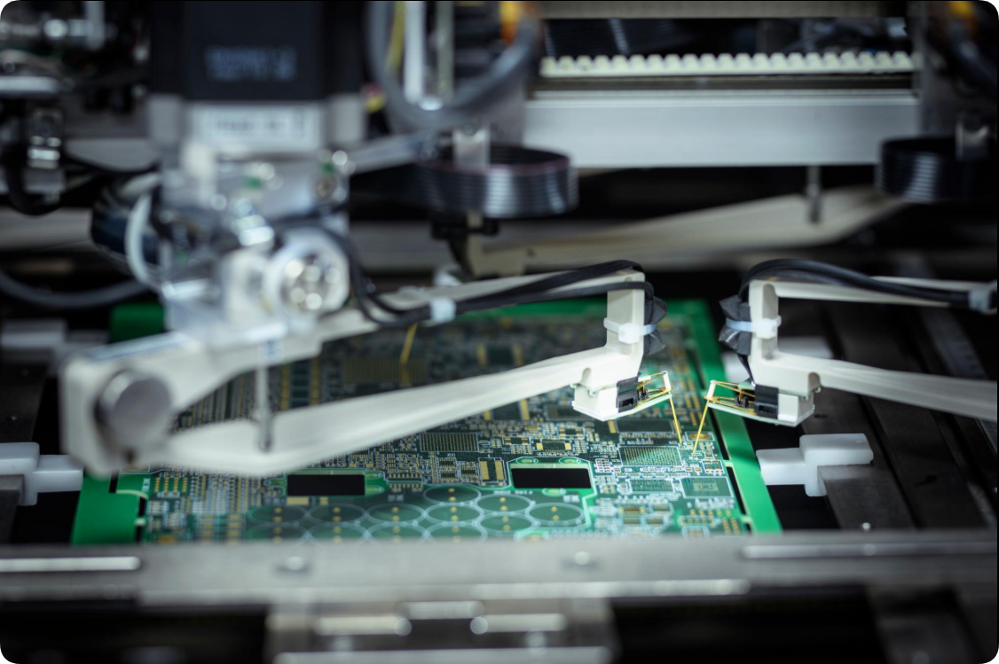
Fig 2 – Flying probe ICT (left) checking shorts and opens; custom FCT fixture (right) simulating industrial I/O signals (24V, RS‑485, CAN)
⚡ 2. Parametric ICT & Dynamic FCT: Electrical Validation Under Real-World Stress
Optical and radiographic metrics verify physical placement and structural uniformity, but they cannot assess silicon performance under electrical loads. NEWEI deploys sequential In-Circuit Testing (ICT) and Functional Testing (FCT) as mandatory electrical validation barriers. For complex, low-to-medium volume industrial control boards, high-precision flying probe ICT stations isolate and measure discrete parametric values—including resistance, capacitance, inductance, diode forward voltage drops, and transistor switching thresholds—without applying operational power to the system architecture. This unpowered testing safely identifies component placement orientation errors, wrong analog values, and micro-shorts before initial power-up.
For high-volume industrial product lines, we design and build dedicated bed-of-nails ICT fixtures capable of testing four identical PCBAs simultaneously. This parallel testing strategy delivers a 400% increase in throughput while maintaining more than 98% component-level fault coverage. Once the board passes parametric ICT, it advances to custom-engineered Functional Testing (FCT) environments.
These specialized FCT fixtures mimic the electrical conditions of the final industrial environment. The system supplies nominal 24V DC operating rails, injects precise analog sensor signals, and drives real-time communication loops across onboard RS-485, RS-232, Modbus, and CAN bus transceivers. For digital and analog I/O modules, the FCT sequencer cycles through every channel under full rated current loads while tracking propagation delays and signal-to-noise ratios. Our production records confirm an unassisted first-pass yield of 97.8% at the ICT stage. Following controlled, IPC-certified rework paths and complete retesting loops, our final combined ICT and FCT yield reaches a consistent 99.4% before packaging.
📋 3. Floor Patrol QC & First Article Inspection (FAI): The Human-Digital Safety Protocol
Automated manufacturing systems require systematic human validation to prevent drift. NEWEI's quality assurance engineers conduct structured, hourly line audits across every active production zone. These patrol procedures verify critical processing variables: solder paste rheology, automated stencil cleaning frequencies, reflow profiling accuracy, ESD ground continuity metrics, and component feeder calibration states. Every floor audit is logged directly into our centralized Manufacturing Execution System (MES) via ruggedized mobile terminals. Any identified variance outside of control limits triggers an immediate line stop for corrective tracking.
To ensure initial process stability, we execute a formal First Article Inspection (FAI) process whenever a new product layout launches, a component batch changes, or an engineering revision occurs. This check requires an exhaustive analysis of the first five boards from the initial assembly run. Our quality lab performs high-resolution dimensional verification with coordinate measuring machines, completes full AOI and AXI cross-checks, analyzes raw ICT/FCT parametric data, and conducts destructive metallurgical cross-sectioning on a sacrificial sample to inspect internal BGA intermetallic compound (IMC) formation layer growth.
We compile these findings into a comprehensive FAI data pack for client review and formal sign-off before releasing the line for volume manufacturing. Over the last 18 months, our pre-FAI validation processes have successfully caught 96% of setup adjustments prior to formal submission, resulting in a 100% acceptance rate for customer-submitted FAIs.

Fig 3 – Defect analysis lab (left) with metallurgical microscope; MES traceability dashboard (right) linking field returns to specific inspection gates
🔁 4. Root-Cause Defect Analysis & Closed-Loop MES Traceability: Engineering Out Failures
When an optical or electrical testing gate flags an anomaly, the affected assembly is routed directly to our dedicated defect analysis lab. Here, failure analysis engineers isolate the root cause using metallurgical microscopes, curve-tracing signature analyzers, and localized X-RAY analysis. Within 24 hours of any recurring fault signature, our engineering team issues a formal 8D problem-solving report that outlines the underlying process root cause—such as localized BGA voiding from solder paste outgassing or connector lead bridging caused by micro-stencil apertures—and implements immediate systemic corrections.
Our quality tracking system monitors the distribution of industrial assembly anomalies to optimize process control: BGA voids exceeding 20% limits comprise 32% of findings; fine-pitch connector pin bridging accounts for 24%; insufficient solder wetting on plated through-hole (PTH) connections represents 18%; surface mount component pick-and-place misalignment makes up 15%; and miscellaneous anomalies fill the remaining 11% variance.
All process observations, testing logs, and component batch codes are written directly into NEWEI's digital MES traceability database. Every completed industrial board features a permanent, laser-etched 2D DataMatrix code that archives its production genealogy: incoming manufacturer lot numbers, paste printing parameters, component placement machine identifier tags, raw 3D AOI/AXI image sets, exact ICT/FCT parametric performance values, authorized rework records, and shipping log files. In the event of a long-term deployment issue, our tracking system can scan the barcode and isolate affected batches, component origins, or production shifts within minutes. This data transparency helps our partners secure long-term capital equipment contracts. Over the past 24 months, these data-driven process adjustments have reduced our total internal defect rate for industrial control hardware from 380 DPPM down to 144 DPPM, marking a verified 62% gain in systemic quality.
📊 Real-Time Manufacturing Metrics: Dedicated Industrial Production Line
We maintain open performance data across our specialized industrial manufacturing cells. The following operating metrics are updated continuously on our floor displays and remain accessible to clients via our secure web portal:
- 3D AOI First-Pass Yield: 96.2% across high-mix industrial product runs.
- AXI Automated Rejection Rate: 0.7% for BGA assemblies exceeding internal 20% voiding caps.
- In-Circuit Testing (ICT) First-Pass Yield: 97.8% verified at parametric check stations.
- Functional Testing (FCT) Final Yield: 99.4% following certified rework pathways.
- Verified 12-Month Field Return Rate: 0.008% (under 80 ppm across active operations).
- Average 8D Engineering Resolution Time: 18 hours from initial fault capture to verified correction.
Secure Long-Term Hardware Reliability For Your Industrial Applications
The long-term reliability of your industrial controller relies on verifiable manufacturing data—including automated X-RAY analysis for every BGA, full functional simulation for every I/O path, and complete traceability tracking for every manufacturing step. At NEWEI, we treat sub-150 ppm defect control as an active daily engineering practice rather than a marketing objective.
Connect With Our Quality Engineering Team:
Direct Phone Support: +86-18925218989
Engineering Inquiries: tiger.wang@richitek.com
Official Platform: https://www.neweiodm.com/
Contact us today to schedule a formal quality facility audit or to request raw AXI, ICT, and FCT data reports for your pending industrial hardware projects.
© 2026 NEWEI Industrial – From raw AOI telemetry to field traceability logs, every industrial assembly is fully documented.
Tags: Industrial PCBA X‑RAY inspection / BGA void defect control /
Next: Why Your Handheld PDA OEM Partner Must Master Packaging, Testing & Global Delivery