Why HDI Multilayer PCB Capability Defines Your Industrial Motherboard & Mini PC Success
My Take: HDI multilayer PCB manufacturing isn’t a question of “can it be done” anymore — it’s a battle of “how dense, how stable, and what yield.” I’ve seen too many clients walk into a factory with a 6-to-12-layer design, only to get stuck on microvia drilling delays or BGA cold joints that scrap entire batches. The real differentiator comes down to mastering microvia laser drilling, stacked/staggered vias, 0201 component placement, and signal integrity. NEWEI’s decade of industrial motherboard ODM experience proves one thing: high-density PCB fabrication is essentially a process prediction game that starts at the design stage.
Why HDI Multilayer PCB Capability Defines Your Industrial Motherboard & Mini PC Success
If your next product runs on an Industrial Motherboard, a compact Mini PC, or a fully customized Custom PC, the PCB inside it is no longer a simple substrate — it’s the nervous system. And when that system demands 6 to 12 layers of high-density interconnect (HDI) with microvias, stacked vias, and buried vias, partnering with a proven Custom PCB Assembly Services provider becomes the single most important decision in your production cycle. The industry is shifting: automotive electronics, industrial IoT gateways, and edge computing servers all require PCBs that pack more functionality into smaller footprints while maintaining signal integrity under harsh conditions. This is not a trend — it’s the new baseline.
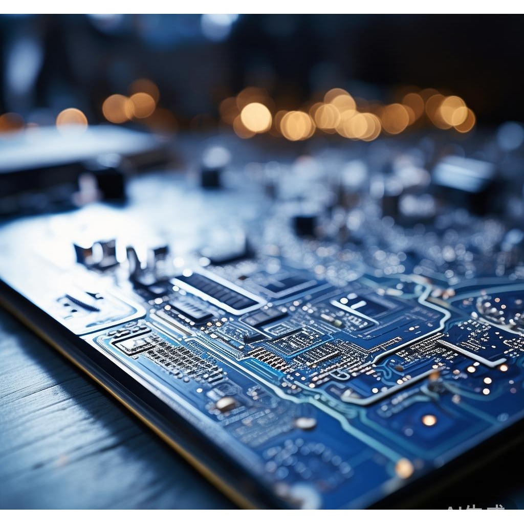
Microvia Laser Drilling & Stacked Via Technology: The Backbone of 6-12 Layer HDI
Anyone can claim they support HDI. But the real test is how they handle microvia laser drilling. At NEWEI, we use UV and CO₂ laser systems capable of drilling microvias with diameters as small as 0.075mm — essential for routing signals between layers in a 12-layer Industrial Motherboard. The real challenge? Maintaining consistent via wall quality across 10,000+ panels without resin smear or copper peel. Our process engineers tune the laser pulse energy and focal position for each dielectric material, whether it’s standard FR4 or high-speed laminates like Megtron 6. For stacked and staggered via structures, we apply a sequential lamination process that ensures every via stack (1+N+1, 2+N+2, or even 3+N+3) passes thermal stress testing at 288°C for 10 seconds. This is what allows a Mini PC to fit a full x86 chipset, DDR5 memory, and multiple M.2 slots into a chassis smaller than a paperback.
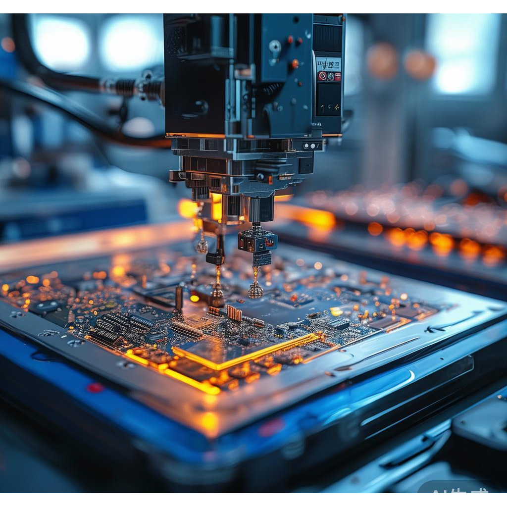
BGA Soldering Yield Control: ±0.01mm Precision Meets X-Ray Validation
BGA packaging is where most PCB assembly projects hit a wall. A 0.4mm pitch BGA with 400+ balls leaves virtually no room for error. NEWEI’s BGA soldering process starts with stencil design — we laser-cut stencils with aperture ratios optimized for each ball diameter, then validate solder paste volume using 3D SPI (Solder Paste Inspection). During reflow, we run a 10-zone convection oven with nitrogen atmosphere to reduce oxidation, and the temperature profile is tailored for each board’s thermal mass. A thick Custom PC board with heavy copper planes demands a slower ramp rate than a thin Industrial Motherboard. After soldering, every BGA goes through X-Ray inspection to check for voids, bridges, and ball coplanarity. Our standard is IPC-A-610 Class 3, meaning we reject any void exceeding 15% of the ball diameter. This level of control is why our custom

ers in industrial automation and medical devices trust us with their most complex assemblies.
0201 Micro-Component Placement & Signal Integrity: The Miniaturization Equation
When your design calls for 0201 (0.6mm × 0.3mm) passive components, you can’t rely on standard pick-and-place accuracy. Our Fuji NXT III and Siemens SIPLACE X4S systems achieve placement accuracy of ±0.02mm at 3 sigma, with a dedicated feeder bank for 0201 reels that minimizes component rotation and tombstoning. But high-density placement is only half the story. On a 10-layer Industrial Motherboard running at 2.5 GHz, signal integrity becomes the bottleneck. We use TDR (Time Domain Reflectometry) to verify differential pair impedance within ±5% tolerance, and run crosstalk simulations during the DFM review phase. For Mini PC designs with USB4 or PCIe Gen5 lanes, we recommend specific stack-up configurations to the customer before production starts — because fixing impedance mismatch after ass
embly is nearly impossible. This proactive engineering approach, combined with our Custom Industrial PC PCBA ODM service, ensures that your high-speed design actually works at scale.
Multi-Product Synergy: How Industrial Motherboard + Mini PC + Custom PC Share One Manufacturing Backbone
One of the most common misconceptions is that different product categories require completely different production lines. In reality, the core technologies — HDI layup, microvia drilling, BGA reflow, 0201 placement, and Class 3 inspection — are identical whether we’re building a rugged Industrial Motherboard for a factory PLC, a fanless Mini PC for a digital signage network, or a fully customized Custom PC with dual GPUs for AI inference at the edge. What changes is the DFM (Design for Manufacturability) checklist. For example, a Mini PC with a height constraint of 20mm forces us to use thinner core materials and buried vias to reduce layer count, while a Custom PC with a high-power CPU requires thicker copper (2oz or more) and thermal via arrays. All of these variations are handled within the same SMT Assembly workflow, with real-time adjustments to stencil thickness, reflow profile, and test coverage. This is what a true one-stop EMS provider should deliver — not just capacity, but adaptability.
Real-World Applications: Where HDI Capability Directly Impacts Product Performance
Let’s look at three scenarios where HDI PCB capability isn’t just a spec sheet checkbox — it’s a competitive advantage:
Industrial IoT Gateway (Industrial Motherboard): A 12-layer HDI board with dual Ethernet PHY, 4G LTE module, and CAN bus interface. The challenge was maintaining isolation between the RF section and digital logic on a 100mm × 70mm form factor. Our solution used a 2+N+2 stacked via structure with buried vias for signal routing, and a dedicated ground plane layer for impedance control. The board passed EMC pre-compliance on the first try.
Edge AI Mini PC (Mini PC): A customer needed a palm-sized PC capable of running YOLOv8 inference at 30 FPS. The 8-layer HDI design packed an Intel N100 CPU, 16GB LPDDR5, and an NPU accelerator. We optimized the BGA fanout pattern for the CPU and used staggered microvias to route the high-speed memory lanes. The final unit achieved a 15% reduction in PCB size compared to the customer’s previous 10-layer design.
Automated Optical Inspection Station (Custom PC): A custom desktop with 4 camera inputs, a frame grabber card, and a real-time controller. The motherboard required 12 layers with controlled impedance for the camera link interface. NEWEI’s Quick Sampling of PCB Circuit Boards service delivered the first 5 prototypes in 7 days, and after validating signal integrity, the customer moved to mass production with zero design changes.
Industry Trends Driving HDI Demand: Automotive, IoT, and Edge Computing
The numbers don’t lie. The global HDI PCB market is projected to grow at a CAGR of 8.2% through 2030, driven by three forces: automotive electrification (ADAS, infotainment, battery management systems), industrial IoT (sensor hubs, gateways, PLCs), and edge computing (AI inference at the device level). These applications demand PCBs that can handle higher frequencies (above 1 GHz), higher current densities (up to 3A per trace), and higher reliability (10+ year lifespan under vibration and thermal cycling). At NEWEI, we’ve already seen a 40% year-over-year increase in 10+ layer HDI projects, with many customers moving from 8-layer to 12-layer designs to integrate more functions without increasing board size. The cost of HDI fabrication has dropped by roughly 15% over the past two years due to improved laser drilling throughput and materials competition, making it accessible even for mid-volume projects (500-2000 units per month). If your product roadmap includes any of these applications, now is the time to qualify a manufacturing partner who can handle the complexity — not just on paper, but on the production floor.
Conclusion: Your HDI Project Deserves More Than a “Maybe”
Building a high-density PCB is not a black box. It’s a predictable, engineered process — if you work with a team that has the equipment, the process control, and the engineering depth to handle it. Whether you’re developing an Industrial Motherboard for a smart factory, a Mini PC for digital healthcare, or a Custom PC for a specialized compute task, NEWEI offers the full stack: from DFM review and SMT Assembly to Class 3 inspection and Industrial PC PCBA ODM. We don’t just build boards — we build confidence. Get in touch for a free consultation and quotation, and let’s turn your HDI design into a production success story.
Company Service Policy: Free consultation and quotation | Custom PCB Assembly from prototype to mass production | ISO certified manufacturing | Worldwide shipping | Dedicated project manager support.
Tags:
Prev: How NEWEI Ensures Delivery Quality for Projector and Rugged Tablet Production
Next: How Advanced SMT Core Technologies Are Reshaping Modern Electronics Manufacturing