How 3D AOI & X‑RAY Detection Drive Zero‑Defect PCBA Manufacturing – A Real‑World Walk Through Newei’s Shop Floor
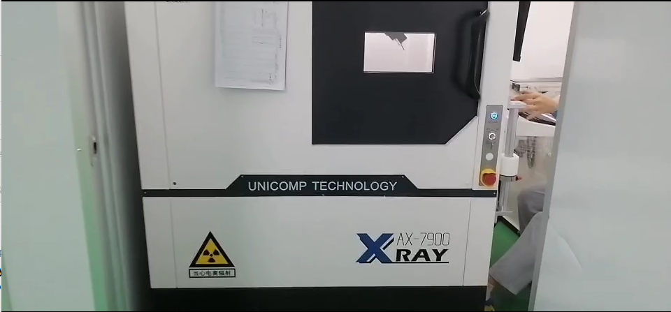
Fig 1 – Our SITAC 3D AOI system inspects every component and solder joint immediately after reflow.
My View: “Trust but verify” is the motto of modern electronics manufacturing. AOI and X‑RAY are not just checkboxes for a quality certificate – they are active process‑control tools. A factory that cannot show you real‑time defect data, classification dashboards, and closed‑loop correction loops is effectively gambling with your product’s reliability.
How 3D AOI & X‑RAY Detection Drive Zero‑Defect PCBA Manufacturing – A Real‑World Walk Through Newei’s Shop Floor
By Newei Industrial (NEWEI) · May 2026
The era of “sample‑based quality control” is over. Today‘s PCBA landscape – with its 01005 passives, 0.4mm‑pitch BGAs, and stacked micro‑vias – leaves no room for guesswork. Zero defects is not a slogan; it is the only viable business model for any EMS provider that serves automotive, medical, or industrial customers. At Newei Industrial, we achieve this through a tightly integrated two‑tier optical and radiographic inspection strategy: 3D Automated Optical Inspection (AOI) followed by Automated X‑RAY Inspection (AXI), backed by relentless defect‑rate tracking and closed‑loop process correction.
First Line of Defense: 3D AOI Inspecting Every Millimeter of Every Board
We deployed online 3D AOI machines at two critical points: immediately after solder paste printing and directly after reflow. The first station – post‑print – measures paste height, volume, and area on every pad. This step alone reduced our solder‑related defects by over 48% because we catch a misaligned stencil or clogged aperture before components are even placed.
The second 3D AOI station (SITAC series, as shown in Fig. 1) scans the whole board after component placement and reflow. Using structured‑light projection and multiple high‑resolution cameras, it reconstructs a true 3D profile of each component and solder joint. It detects lifted leads, tombstoned passives, insufficient heel fillets, and solder bridges – all in less than 25 seconds per panel. False‑call rates are below 0.8%, thanks to our machine‑learning‑trained library database that we have built over 100,000+ production runs.
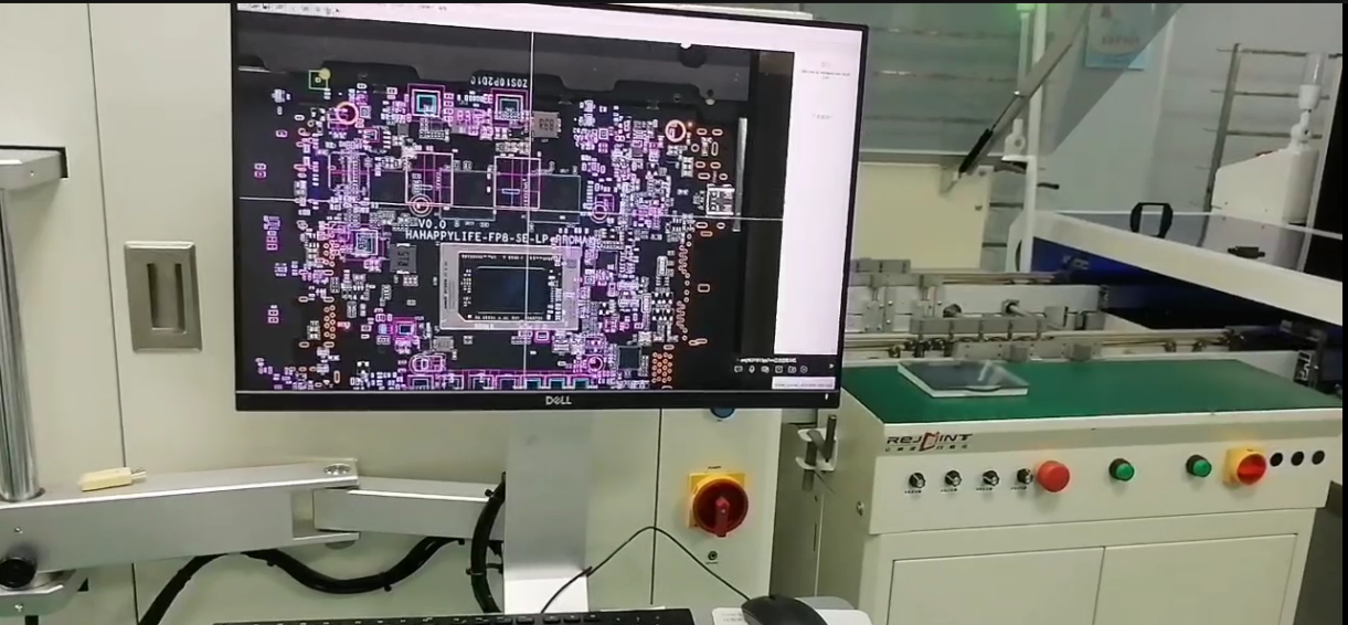
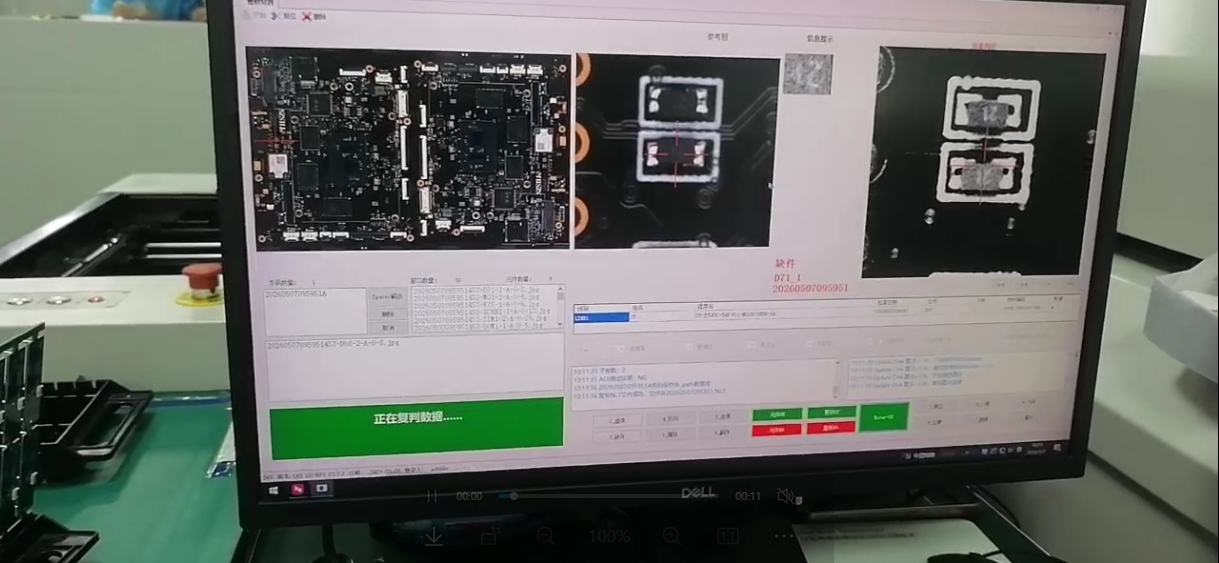
Fig 2 – Our AOI defect Pareto dashboard (live data). Bridges, missing components, and insufficient solder are the top three categories, each addressed by weekly process reviews.
Real Defect Rate Data: Where We Stand in 2026
Transparent data is our contract with customers. Here are our actual rolling‑year defect rates (DPPM) for our high‑reliability product line:
- Solder paste printing (post‑print 3D AOI): 187 DPPM – defects caught and corrected before component placement.
- Post‑reflow 3D AOI (visible defects): 312 DPPM – dominated by minor bridging and part shifts, all routed to real‑time rework stations.
- X‑RAY inspection (hidden defects): 94 DPPM – mainly BGA voids exceeding 25% of ball volume and QFN side‑wetting issues.
Our overall final electrical test yield for boards that pass both AOI and X‑RAY is 99.36% for first‑pass (Class II products) and 98.85% for Class III (automotive/aerospace). Every defect that escapes the optical inspector is captured by X‑RAY; every defect that reaches functional test triggers a full root‑cause loop.
Why X‑RAY Is Non‑Negotiable for Hidden Solder Joints
BGA, LGA, and QFN packages hide their connections under the component body. No amount of lighting or camera angle can visualize those joints externally. This is why we integrated a high‑resolution automated X‑RAY inspection system (AXI) directly after the reflow oven and before ICT. The AXI uses a micro‑focus X‑ray tube (5‑8 µm spot size) and a digital flat‑panel detector. It tilts the board up to ±70° to look at each solder ball from multiple angles, detecting:
- Void percentage – IPC‑A‑610 classes: < 25% void acceptable for most; our internal spec is < 20% for automotive work.
- Head‑in‑pillow (HIP) defects – where the ball and paste never properly coalesce.
- Internal cracks / micro‑shorts caused by mechanical stress during handling.
- Insufficient wetting under large exposed pads – especially for power QFNs.
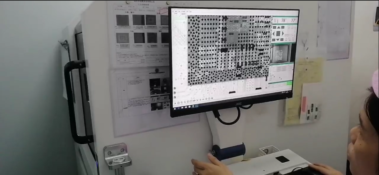
Fig 3 – Our X‑RAY inspection station: the board is tilted up to 70° to reveal hidden BGA soldering quality.
From Unchecked Data to Continuous Improvement: The Closed‑Loop Workflow
Our quality system is not a museum of old charts; it is a living process. Every Monday morning, the production and QA teams hold a 40‑minute defect‑review meeting. The Pareto from the AOI and X‑RAY dashboards drives the agenda. If we see a spike in “insufficient solder” on a specific product, we check the stencil printer – maybe the under‑wipe frequency needs adjustment. If BGA void percentages rise, we run a reflow profile study – perhaps the pre‑heat ramp is too aggressive.
We also share anonymized defect summaries with customers who want to understand our manufacturing stability. For one German automotive ECU project, we lowered overall DPPM from 1082 to 346 over six months by acting on AOI/X‑RAY trend data – and our customer rewarded us with a Preferred Supplier Award.
The Complete Inspection Flow: Step by Step
Here is how a typical high‑mix board moves through our QC gates:
- Incoming component verification – visual+RFID scan (no defects pass).
- 3D AOI after solder paste printing – immediate rejection of misaligned deposits.
- Component placement (2 high‑speed SMT lines) – no inspection yet, but all feeders are optically verified.
- 3D AOI after reflow #1 (top side) – full 3D scan; repair flags issued within 5 seconds.
- Second‑side printing + placement + reflow – repeat of steps 2‑4.
- Automated X‑RAY inspection (AXI) – 100% inspection of all BGA, QFN, and shielded components.
- In‑circuit test (ICT) – electrical verification; only boards that pass AOI+X‑RAY enter ICT.
- Functional test (customized test benches) – final sign‑off before packaging.
All inspection data – images, defect codes, timestamps, operator names – are stored in our MES (Manufacturing Execution System). A customer can request a full traceability report for any batch, including the X‑RAY images of their specific boards.
Conclusion: Quality Is Not an Accident
At Newei Industrial, we have built our reputation on being a one‑stop PCBA manufacturer that delivers custom PCB assembly, SMT, and turnkey EMS services with uncompromising quality. The AOI and X‑RAY infrastructure we just described is not hidden behind a glossy brochure – it runs 7 days a week, 22 hours per day, and you are welcome to stand beside our operators and watch the screens populate with real‑time yields.
Newei Industrial (NEWWEI) – your partner for high‑reliability, zero‑defect PCBA. Whether you require quick‑turn prototypes or high‑volume production with full traceability, our engineering team will design a custom inspection plan tailored to your IPC class and test coverage needs. Contact us for a factory audit or a DFM review.
Contact NEWWEI (Newei Industrial)
Web: https://www.neweiodm.com/
Email:tiger.wang@richitek.com
Tags: 3D AOI inspection / X‑RAY inspection PCBA / one‑stop PCBA manufacturer /