How We Track Down Hidden Defects: A Full Walkthrough of Our PCB Assembly Fault-Finding Process
How We Track Down Hidden Defects: A Full Walkthrough of Our PCB Assembly Fault-Finding Process
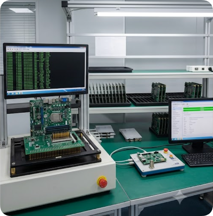
After fifteen years in electronics manufacturing, I can tell you this: no matter how perfect your production plan looks on paper, it means nothing if a single faulty board slips through to a customer. That is why at NEWEI, our PCB Assembly fault-finding process is built as a disciplined, multi-layered system—designed to catch even the smallest anomaly before it becomes a field failure. Whether we are building a complex industrial motherboard or a compact rugged tablet, every board enters our Custom PCB Assembly Services workflow from the moment the first component touches the pad. Let me walk you through how we actually troubleshoot and eliminate defects across the entire production flow, step by step.
My perspective: Most contract manufacturers treat fault-finding as a reactive step—find a bad board, scrap it, move on. That’s not quality control; that’s sorting. Real fault-finding means understanding the root cause, feeding that data back upstream, and preventing recurrence. Our process is built on that feedback loop, and it’s why our defect rates stay in the parts-per-million range, even on high-mix, low-volume runs.
Stage One: First Article Inspection – Catching Misalignment Before It Multiplies
Every production run at NEWEI starts with a First Article Inspection (FAI). This isn't a quick glance; it's a full dimensional and electrical check of the first assembled board against the Gerber files and BOM. For a custom SMT Assembly run on a dense industrial motherboard, our technicians verify pad alignment, solder paste volume, and component polarity under magnification. If the SPI (Solder Paste Inspection) system flags a slight offset on a 0201 resistor, we halt the line immediately. That single correction prevents hundreds of faulty boards downstream.

Stage Two: AOI and X-Ray – Seeing What the Human Eye Misses
Automated Optical Inspection (AOI) scans every solder joint on every board after reflow. For standard components, AOI catches tombstoning, bridging, and insufficient solder. But for hidden joints—like those under a BGA package on a rugged tablet mainboard—AOI can’t see through the chip. That’s where X-Ray inspection steps in. Our operators analyze X-Ray images for voids, shorts, and cold solder balls inside the BGA array. We pair this with our automotive-grade PCBA inspection standards, which demand void areas under 15% for critical power ICs. If the X-Ray shows a void cluster near a thermal pad, the board is flagged for rework or scrap, depending on severity.
Stage Three: ICT and Functional Test – Validating Every Circuit Path
In-circuit testing (ICT) checks each component's value, orientation, and connectivity using a bed-of-nails fixture. For a handheld game console PCBA, the ICT fixture probes over 200 test points in under 30 seconds, measuring resistor values, diode drops, and capacitor ESR. Any deviation outside the specified tolerance triggers an immediate printout of the failing node. After ICT, each board moves to functional test (FCT), where it's powered up and run through a sequence simulating real operation. For a bluetooth thermometer assembly, FCT checks sensor readout accuracy, BLE pairing, and battery charging circuitry. Only boards that pass both ICT and FCT move to packaging.
Inspection Method Comparison
| Method | What It Detects | Stage | Typical Defect Rate Caught |
|---|---|---|---|
| SPI | Solder paste volume, offset | Pre-reflow | ~95% of paste defects |
| AOI | Tombstoning, bridging, insufficient solder | Post-reflow | ~85% of visible joint defects |
| X-Ray | BGA voids, hidden shorts, cold balls | Post-reflow | ~99% of hidden joint defects |
| ICT | Component value, orientation, connectivity | Post-assembly | ~90% of component-level faults |
| FCT | Full system functionality | Final test | ~98% of operational defects |
Combining Products and Services for a Complete Fault-Proof System
What makes our fault-finding process effective isn’t any single machine—it’s how we combine products and services into a unified flow. Take a project where we build a rugged tablet and its companion industrial motherboard. The motherboard goes through SMT Assembly with SPI and AOI, then the tablet’s display assembly passes through our PCBA Three-Proofing line to protect against moisture and dust. Both boards are then tested together in a system-level functional test that simulates field conditions—vibration, temperature cycling, and ESD strikes. If the tablet’s touch controller fails during the cold cycle, we trace it back to a solder joint on the motherboard’s connector. That feedback loop lets us adjust reflow profiles for the next batch. This cross-product, cross-service integration is what turns fault-finding from a gate into a continuous improvement engine.
Real-World Scenarios: Where Fault-Finding Makes or Breaks Delivery
Here are five common scenarios where our process has directly prevented field failures:
Automotive electronics – An industrial PC PCBA for a fleet management system failed ICT due to a swapped capacitor value. Our FAI caught it before the first production board left the line.
Smart home devices – A bluetooth speaker assembly showed intermittent audio dropouts in FCT. X-Ray revealed a hairline crack in a crystal oscillator joint; we corrected the reflow profile.
Medical IoT – A bluetooth thermometer prototype had inconsistent BLE range. Our RF testing team traced it to an antenna matching network mismatch and reworked the design.
Industrial handhelds – A handheld PDA batch failed ingress testing. Three-proofing inspection found uneven conformal coating on the USB port area; we retrained the coating operator.
Consumer gaming – A handheld game console had a 2% failure rate on the audio jack during FCT. We discovered the jack's solder pads were undersized in the original design and issued a PCB revision.
Building a Culture of Traceability and Root Cause Analysis
Every board that fails any test stage gets a unique defect tag in our MES system. The tag includes the operator ID, machine ID, reflow profile, and time stamp. Our quality engineers review defect trends weekly. If we see a spike in tombstoning on a particular PCB Manufacturing batch, we correlate it with the paste printer’s stencil tension readings and the component supplier’s lot code. This level of traceability lets us pinpoint whether the issue is process-related, material-related, or design-related. For example, when we noticed an uptick in BGA solder ball voids on one SMT Assembly line, we traced it to a worn-out nozzle on the pick-and-place machine. Replacing the nozzle solved the problem in under an hour. That’s the difference between just testing and truly controlling quality.
Your Partner in Zero-Defect PCB Assembly
Fault-finding isn’t just about catching bad boards; it’s about building a system that makes bad boards rare. At NEWEI, we combine rigorous inspection, cross-service integration, and deep traceability to deliver PCB Assembly (PCBA) that you can trust from prototype to mass production. Whether you need a rugged tablet with conformal coating or an industrial motherboard with full ICT coverage, we’re ready to learn more about our manufacturing capabilities and discuss your next project. Contact us today for a free consultation and quote—your product deserves a partner that finds faults before they find your customers.
Tags: PCB fault finding /SMT quality inspection /PCBA testing /AOI X-ray PCB /
Prev: How Factory Culture Shapes Reliable Custom PCB Assembly & Electronics Manufacturing Services