
Common SMT and DIP Assembly Defects and How to Troubleshoot Them
Every contract manufacturer eventually hits the same wall: a board that cleared visual inspection but failed functional test, or a batch where tombstones appear on one line and not the next. In high-mix production the gap between a stable yield and a runaway rework queue usually comes down to how fast you can read a defect and trace it to its root cause. This article walks through the failure modes we see most often in SMT Assembly and DIP Assembly, plus the practical fixes that keep them from returning. When the same product is built under a full EMS Electronic Manufacturing program, the same logic simply scales across more lines and more part families.
In my experience, most teams over-invest in inspection and under-invest in the stencil and the reflow profile. You can buy the best AOI machine on the market, but it will not fix solder paste that was already wrong before it touched the pad. Treat the print and the thermal profile as the two load-bearing walls of your process, and troubleshoot there first. Inspection tells you what broke; the stencil and the oven tell you why.
💡 Why SMT Assembly Yield Starts at the Stencil
The single biggest lever in surface-mount work is the print. A solder paste deposit that is too thick, misaligned, or starved will produce defects no amount of downstream correction can save. That is why our line engineers treat the stencil aperture and the squeegee pressure as the first place to look whenever a new professional SMT Assembly job starts throwing failures. Getting the deposit right at 0.1 mm pitch is not magic; it is a repeatable set of tolerances you can verify in minutes.
Solder Bridging Between Fine-Pitch Pads
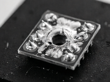
Bridging shows up as a thin web of solder shorting two adjacent leads, most often on QFP and connector footprints. The usual culprit is aperture opening wider than the pad, or a stencil that has begun to smear paste at the edges. Walk the board under a microscope and you will typically find the bridge sitting on the inner corners where the deposit was heaviest. The fix is rarely a slower conveyor; it is a tighter aperture, a stepped stencil for mixed-density boards, and a verify-print inspection right after the printer. We also check the paste roll and the separation speed, because a snappy snap-off leaves a cleaner brick than a hesitant one.
Tombstoning and Head-in-Pillow
Tombstoning is the classic one-legged component standing on end, and it almost always points to an unbalanced reflow. If one pad wets a fraction of a second before the other, surface tension pulls the part upright. The remedy is a reflow profile with a gentle soak zone so both terminations reach liquidus together, plus tighter paste volume control so one side is not starving. Head-in-pillow is subtler: the ball and the pad each form their own oxide skin and never truly fuse, passing visual check but failing at temperature cycling. Lowering the ramp rate and confirming the BGA has a clean, flat coplanarity before placement is what resolves it. These are profile problems before they are placement problems.

🏭 Reading DIP Assembly Failures After Wave Soldering
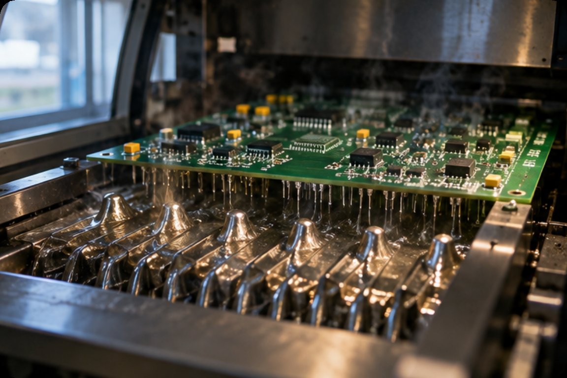
Through-hole work hides a different class of problems. Once a board leaves the wave, the defects are larger, more visible, and usually tied to how the flux, the preheat, and the wave contact time were balanced. A competent DIP Assembly cell treats the wave as a system, not a single event, and logs every parameter shift so a bad run can be reconstructed later.
Cold Joints and Insufficient Wetting
A cold joint looks dull and grainy, and it fails mechanically long before it fails electrically. The root cause is almost always insufficient preheat: the board hits the wave too cold, the solder freezes before it can wet the lead, and you get a joint that looks attached but is not metallurgically bonded. Raising the preheat to bring the laminate to a stable 100 to 120 degrees Celsius before contact fixes most of these. We also watch the conveyor angle; a slightly steeper entry reduces shadowing behind tall components and lets the wave wrap the lead instead of skipping it. When wetting is weak across a whole panel, suspect the flux activity or a contaminated wave pot before you suspect the operator.
Solder Balls and Icicles
Solder balls scattered near through-hole joints and icicles hanging off leads are both signs of turbulence at the wave exit. Balls form when paste spatter or trapped gas ejects tiny droplets, while icicles are the wave tearing as the board lifts away. The cure is a cleaner exit with the correct conveyor speed and a modest reduction in wave height so the separation is smooth rather than violent. Wave soldering is sensitive to board layout too; wide copper pours act as heat sinks that pull the joint temperature down, so we often ask design to balance the thermal mass before we touch the machine settings. Most icicle complaints disappear once the layout and the exit geometry agree.
A Field-Tested Inspection Workflow for Line Engineers
Good troubleshooting is not heroics; it is a gate strategy that catches the right defect at the right stage. We use three gates so that no single failure has to travel far before someone sees it, and so that the data builds a pattern you can act on.
Three-Stage Gate Strategy
The first gate is print verification, where a 2D or 3D inspection confirms deposit volume and alignment before placement. The second is post-reflow AOI, which flags bridging, missing parts, and polarity. The third is a functional or in-circuit test that proves the board actually works, not just that it looks right. Each gate feeds a defect Pareto back to the process owner, which is how a repeating tombstone problem gets traced to a profile shift instead of being reworked blind. When the program runs as part of a broader SMT Assembly and through-hole mix, the same three gates cover both technologies with one reporting layer.
| Process | Best Suited For | Primary Defect Focus |
|---|---|---|
| SMT Assembly | High-density, fine-pitch, and BGA boards | Bridging, tombstoning, head-in-pillow |
| DIP Assembly | Connectors, transformers, and power components | Cold joints, icicles, insufficient wetting |
| EMS Electronic Manufacturing | Full turnkey programs with mixed technology | Cross-stage yield and traceability |
Choosing the Right Process Partner for Your Boards
Defect control is partly your own discipline and partly the capability of the shop building the board. A partner who documents every stencil, profile, and wave setting gives you a feedback loop; a shop that treats each run as a fresh guess leaves you debugging the same problem every quarter. The value of a mature EMS Electronic Manufacturing relationship is that the troubleshooting knowledge compounds instead of resetting.
Before you commit a volume order, ask to see the process window documentation for the specific package you use most, whether that is a 0.4 mm QFP or a heavy through-hole power section. A credible supplier will show you the reflow profile and the print tolerance they hold, not just a pass rate. The cheapest quote rarely survives contact with a tricky laminate, and the cost of a field return dwarfs the savings of a skipped inspection gate. Build the partnership around shared data, and the defects that used to surprise you become items you caught at gate one.

The takeaway is straightforward. Most SMT and DIP failures are not random bad luck; they are the predictable result of a print, a profile, or a wave setting drifting outside its window. Inspect early, trust the data, and put your troubleshooting effort where the process is actually made or broken. Do that consistently and your rework queue shrinks, your functional yield climbs, and your customers stop calling about boards that looked fine but were not.
Tags: SMT assembly defects / DIP wave soldering / EMS manufacturing quality /
Prev: How PCBA Three-Proofing Paint Cut Field Failures for a Medical Device OEM
Next: Why Custom Automotive Electronics Is Reshaping Customer Case Programs in 2026