99.99% SMT Yield in Mini PC Production: Inside 0201 Micro-Pitch Placement, BGA Soldering & DIP Wave Soldering

Here’s something I've learned after years on the factory floor: hitting 99.99% first-pass yield on 0201 micro-pitch SMD placement isn't about luck or a single miracle machine. It’s a ruthless discipline built into every gram of solder paste, every micron of stencil alignment, and every thermal degree of a reflow profile. When we produce mini PC motherboards for edge AI, digital signage, and industrial IoT, we aren’t just assembling boards — we’re guaranteeing a process window where BGA soldering void rates stay below 5% and SPI inspection catches shape deviations before they become field failures. I’ve seen too many fabs chase placement speed while ignoring solder paste rheology and wave soldering thermal balance. That’s why I’m putting our real production footage under the microscope. No marketing fluff — just the hardcore process control that keeps our mini PC SMT line at the top.
1. Solder Paste Printing & SPI Inspection: The Invisible Foundation
Most people fixate on the fast-moving placement heads, but in a high-mix SMT line, the battle is won or lost at the stencil printer. For 0201 micro-pitch components and 0.4mm pitch BGAs, we use laser-cut stainless steel stencils with nano-coating, running on fully automatic printers that control squeegee pressure within ±1 N. The solder paste itself is a Type 4.5 no-clean formulation, optimized for humidity ranges from 35% to 65% RH. Why does this matter? The explosion of edge AI mini PCs and embedded industrial controllers means boards are denser than ever. A single insufficient paste deposit on a BGA pad can trigger intermittent opens that only appear after thermal cycling.
Right after printing, our 3D SPI (Solder Paste Inspection) system measures volume, area, height, and offset for every pad — at a speed matching the high-speed pick-and-place rhythm. We enforce a strict tolerance: volume variation below ±15% for 0201 pads, and below ±10% for BGA spheres. If an anomaly is flagged, the line pauses automatically. I’ve watched real-time SPI trend charts catch a slightly worn stencil blade before it produced a single bad board. That’s not just inspection; it’s predictive process control. For anyone building IoT gateways or digital signage players that must run 24/7 without reboot, this level of print integrity isn’t optional — it’s the difference between a five-year life and a six-month RMA headache.
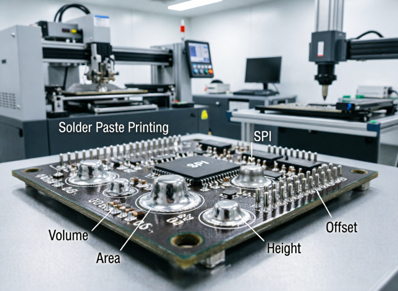
Fig. 1 – Automatic solder paste printing with downstream 3D SPI analysis. Every deposit on a mini PC board is measured for volume and alignment before a single component is placed.
2. High-Speed Pick-and-Place for 0201 & Micro-Pitch SMD
When you watch a high-speed SMT pick and place machine running at full speed, the motion is almost hypnotic — multiple placement heads moving in perfect synchronization, placing over 45,000 components per hour. For our mini PC boards, a single PCB might carry more than 280 0201 chip resistors and capacitors alongside fine-pitch QFN and BGA packages. The placement accuracy required is ±25 µm at Cpk ≥ 1.67. To maintain 99.99% placement yield on such tiny parts, we use dual-camera alignment on every component and closed-loop servo feedback that compensates for thermal drift across an 8-hour shift.
I want to emphasize a point many overlook: 0201 micro-pitch reliability hinges on pad design and component spacing, not just machine specs. Our land patterns follow IPC-7351B but with modified toe and heel fillets derived from hundreds of cross-section analyses. This becomes critical as AI-accelerated mini PCs adopt LP-DDR memory down and complex PMIC layouts. When a product is destined for factory automation or retail kiosk environments, vibration and temperature swings constantly test those solder joints. The 99.99% first-pass yield figure isn't a marketing badge — it’s a statistical guarantee that we’ve eliminated placement-related defects to fewer than 10 defects per million opportunities. And yes, that requires auditing every feeder calibration every four hours. No shortcuts.
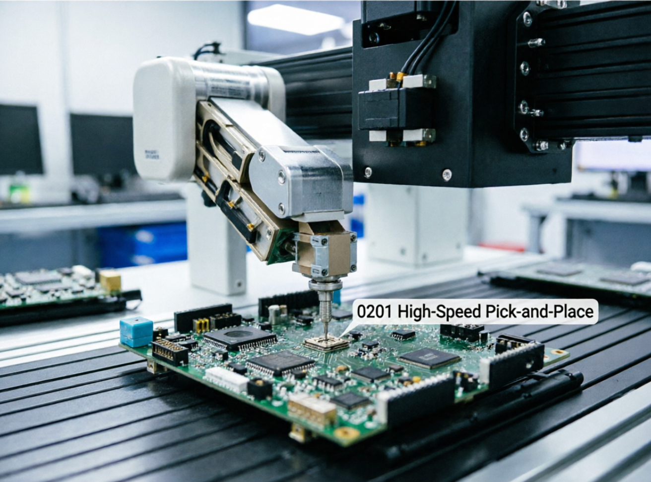
Fig. 2 – High-speed placement head in action, mounting 0201 chip components on a mini PC motherboard. Dual-camera alignment ensures ±25µm accuracy at full speed.
3. BGA Soldering & Reflow: Mastering the Heat
If 0201 placement tests mechanical precision, BGA soldering tests thermal engineering. Our mini PC designs frequently use 0.5mm and 0.4mm pitch BGAs for CPUs, FPGAs, and wireless modules. Achieving void-free joints and intermetallic layer thickness between 1–2 µm requires a reflow profile that’s tweaked for each board’s thermal mass — not just a generic ramp-soak-spike curve. We deploy 10-zone convection reflow ovens with real-time profiling on a sacrificial coupon for every batch. Nitrogen atmosphere keeps oxygen levels below 500 ppm, drastically reducing dross and improving wetting on lead-free SAC305 alloys.
Why so much attention to BGA process details? Because the hottest product categories — ultra-compact mini PCs for edge computing, medical panel PCs, and in-vehicle embedded systems — operate in thermally unforgiving corners. A cracked BGA ball under a heatsink isn't just a manufacturing defect; it's a ticking clock. We cross-verify with X-ray inspection and, for mission-critical runs, acoustic microscopy. My personal rule: if a BGA shows more than 8% void area in the critical outer row, the profile gets adjusted. This level of scrutiny is what separates high-yield SMT factories from hobbyist lines. When a customer plugs in a fanless industrial mini PC inside a hot factory, they should never have to think about the solder joints underneath that processor. Our job is to make sure they never do.
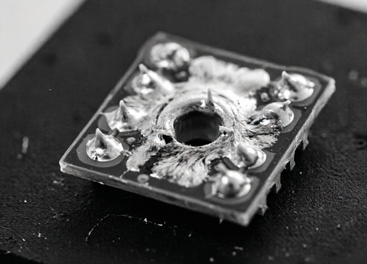
Fig. 3 – X-ray inspection of BGA solder joints after reflow. Void analysis and intermetallic consistency are verified before boards move to DIP assembly.
4. DIP Through-Hole & Wave Soldering: Where Legacy Meets New Demands
A mini PC motherboard isn’t all surface mount. Through-hole connectors, USB-C receptacles, audio jacks, power barrel connectors, and large capacitors still rely on the DIP (Dual In-line Package) insertion and wave soldering process. And here’s where cross-process discipline counts: you can have a perfect SMT side only to ruin it with improper wave flux application or incorrect preheat. Our DIP line integrates automatic insertion machines for large pin counts, with operators following standardized work instructions that detail insertion angles, clinch lengths, and even glove change frequency to avoid contamination.
During lead-free wave soldering, we maintain pot temperature at 260±3°C, using a dual-wave system that ensures proper hole fill on thick multi-layer PCBs. Conveyor speed and preheat temperatures are locked to board-specific recipes, stored via barcode scanning. The cross between SMT and DIP is where many mini PC products fail — paste residues from reflow can interact with wave flux, creating blowholes. Our solution: strict board cleaning protocols and flux compatibility testing baked into NPI. Given the booming demand for IoT edge servers, retail POS systems, and laboratory automation mini PCs, the mix of high-density SMT and robust through-hole connectors is what makes these products durable enough for 10-year deployments. You can’t just nail the 0201 placement and ignore the DIP side. I’ve observed that top-tier manufacturers treat the entire SMT-to-wave continuum as one interdependent system — and that’s exactly how we operate.

Bringing It All Together: Process Integration & Industry Pulse
Walk through our facility and you’ll see the synchronization: SPI data feeds into the placement optimizer; reflow logger data adjusts the printer's next cycle automatically; wave solder throughput aligns with SMT output to prevent WIP buildup. The products on these lines mirror what’s hot right now — Mini-STX form factor PCs for digital signage, embedded AI inference boxes with integrated NPUs, and ultra-rugged industrial controllers that run on Linux at the edge. These applications demand manufacturing traceability down to the individual component reel. We log every placement event, every SPI image, and every wave solder thermal trace, tying it to the board’s serial number. In my view, this is the real moat. Anyone can buy the same brand of placement machine; not everyone builds the data ecosystem to consistently hit 99.99% SMT yield on a mixed 0201, BGA, and DIP board.
The next wave — Industry 4.0 gateways, smart city nodes, autonomous mobile robot controllers — will shrink board sizes even further, pushing more manufacturers toward 01005 passives and system-in-package assemblies. But the fundamentals won’t change: control the printing, nail the placement, refine the thermal profile, and never let the DIP tail wag the SMT dog. I hope this inside look at our mini PC SMT production and DIP wave soldering operations proves that yield is a culture, not a KPI.
Want to discuss your mini PC motherboard requirements or see our 0201/BGA process in person? Contact our engineering team →
Tags: high-mix SMT line /BGA soldering /mini PC manufacturing /
Prev: Eliminating BGA Soldering Defects: A Deep Dive into HIP, Voids, and Process Optimization
 in PCBA processing")