Eliminating BGA Soldering Defects: A Deep Dive into HIP, Voids, and Process Optimization
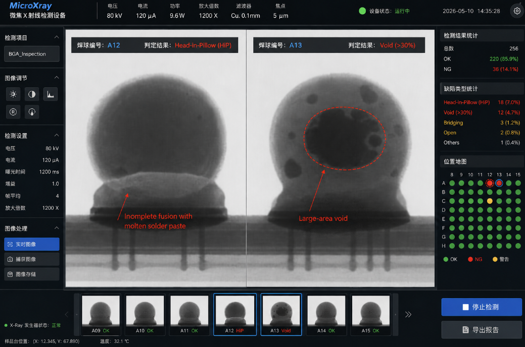
Fig 1 – High-resolution X-Ray inspection: Identifying the critical "Head-in-Pillow" effect and volumetric voiding issues in high-density PCBA.
Engineer's Perspective: The Physics of Reliability
After a decade on the SMT floor, I've realized BGA (Ball Grid Array) assembly is less about "soldering" and more about managing thermal dynamics. When you deal with 0.5mm pitches and thousands of joints per board, a variance of just $5^{\circ}C$ in your reflow profile isn't just a statistic—it's a potential field failure. This guide distills our team's frontline experience in achieving a 99.5% first-pass yield by mastering the bridge between IPC standards and real-world manufacturing physics.
Eliminating BGA Soldering Defects: A Deep Dive into HIP, Voids, and Process Optimization
Technical Report by NEWEI Industrial Engineering Team · Updated May 2026
As global demand for high-performance computing (HPC) and AI-driven automotive systems skyrockets, the BGA package market is surging toward a $45 billion valuation by 2028. However, the complexity of these components remains a bottleneck. Industry data suggests that 65% of intermittent hardware failures originate from invisible BGA defects like Head-in-Pillow (HIP) or micro-cracking.
At NEWEI, our engineering department—boasting an average of 12 years in SMT troubleshooting—has refined the BGA assembly process through over 200 high-stakes cases. We don't just follow IPC-A-610 Class III; we exceed it using vacuum-assisted technologies and advanced metrology.
🛡️ 1. Solving the "Head-in-Pillow" (HIP) Phenomenon
HIP is the "phantom" defect of SMT. It occurs when the BGA ball and the printed solder paste melt independently but fail to merge. The result is a physical contact that passes electrical testing but fails under the slightest mechanical or thermal stress.
- Root Causes: PCB dynamic warpage during reflow, flux exhaustion in the soak zone, or oxidation on the BGA spheres.
- The NEWEI Solution: We implemented Vacuum-Assisted Reflow (VAR). By maintaining board flatness and removing oxygen during the liquidus stage, we reduced dynamic warpage from 0.15mm to less than 0.05mm. Switching to a high-activity, wide-window flux ensures the "marriage" of the ball and paste even during extended thermal cycles.
🫧 2. Mitigating Excessive Solder Voids
While IPC-A-610 allows for 25% voiding by area, automotive and medical sectors often demand much stricter limits. Voids act as stress concentrators, leading to crack propagation over time.
Our Advanced Protocol: To meet the<10% voiding requirements for power-integrity balls, we utilize a 30-second vacuum dwell at peak temperature. This literally sucks out gas bubbles (outgassing from flux or PCB moisture) before the solder solidifies. For sensitive substrates, we optimize the soak ramp to $0.9^{\circ}C/sec$, allowing volatiles to escape gradually without creating turbulence in the molten joint.
⚡ 3. Non-Wet Opens & Solder Splashing
Non-wet opens (NWO) occur when the solder fails to "grip" the pad, often due to microscopic oxidation. Conversely, solder splashing (beading) is caused by aggressive preheating that causes flux to "pop," throwing solder particles across the board.
Plasma Surface Treatment: We utilize atmospheric plasma cleaning on BGA pads to remove organic residues, improving the wetting angle by roughly 40%.
Stencil Engineering: We've transitioned to electroformed stencils with hexagonal apertures. This improves paste release (Transfer Efficiency) to 89% for 0.4mm pitch components.
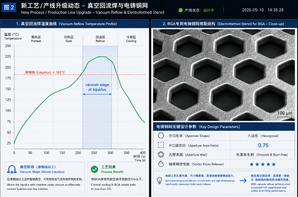
Fig 2 – Left: Optimized thermal profile featuring a vacuum degassing phase; Right: Laser-cut stencil geometry for precision paste volume control.
📐 Quality Benchmarks: NEWEI vs. Industry Standards
Consistency is born from rigor. Our internal thresholds are intentionally set tighter than international standards to provide a safety buffer for our clients.
| Metric | IPC-A-610 Class III | NEWEI Internal Spec |
|---|---|---|
| Max Void Area | 25% | 20% (10% for Power) |
| Allowable Warpage | 0.75% of Length | Max 0.05 mm/inch |
| Inspection Method | 2D X-Ray / Visual | 3D X-Ray (AXI) + Cross-sectioning |
🔬 Continuous Innovation in 2026
We don't believe in "set and forget." Our facility has recently integrated Shadow Moiré technology to track real-time warpage during the actual heating cycle. This allows our engineers to customize PCB support structures for every batch, effectively neutralizing the mechanical stress that leads to micro-cracking.
Additionally, our AI-Assisted X-Ray Analytics now autonomously grades every solder joint against our historical database of 1,200+ unique BGA profiles, ensuring that human fatigue never impacts quality assurance.
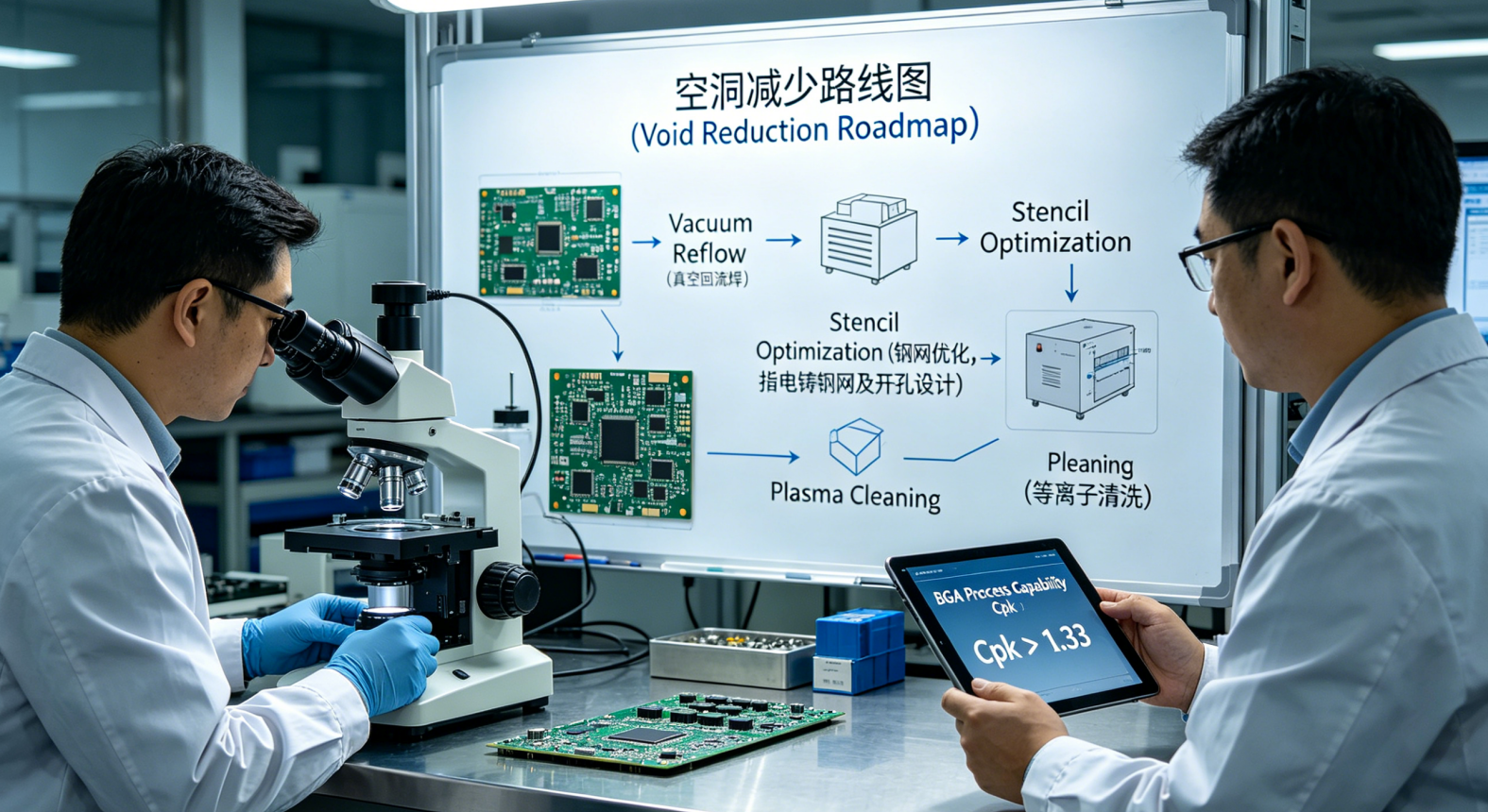
Fig 3 – Our engineering leads analyzing cross-sectional micrographs to validate the integrity of internal grain structures in lead-free solder balls.
🚀 Summary: Why Process Maturity Matters
The transition from a 96% yield to a 99.5% yield represents more than just cost savings—it represents brand protection. In the high-stakes world of medical electronics and automotive sensors, a single BGA failure is one too many. NEWEI’s combination of vacuum reflow, plasma cleaning, and AI inspection provides a multi-layered defense against the industry’s most common failures.
Partner with BGA Specialists
Leverage our 12+ years of SMT expertise for your next project. We provide full transparency—from void data reports to DFM feedback.
NEWEI Industrial (Newei ODM)
📍 Shenzhen, China
🌐 www.neweiodm.com/
📞 Direct: +86-18925218989
📧 Email: tiger.wang@richitek.com
READY FOR A DFM REVIEW? SEND YOUR BOM TODAY.
© 2026 NEWEI Industrial. All Rights Reserved. Specializing in high-density PCBA, Vacuum Reflow, and Advanced BGA X-Ray Inspection Services.
Tags: BGA soldering defects / head‑in‑pillow solution / vacuum reflow BGA /
Prev: Survival of the Leanest: Why Newei is Rewriting the SMT Assembly Playbook for the AI Hardware Era