
Real-World Data: How Custom PCB Assembly Quality Control Impacts Your Product's Failure Rate in 2025
Real-World Data: How Custom PCB Assembly Quality Control Impacts Your Product's Failure Rate in 2025
Let me be direct with you: the biggest cost in electronics manufacturing isn't the components or the labor—it's the rework. When you source a custom PCB assembly partner, every defect that slips through their quality control becomes your field failure. And field failures kill brands. I've spent over a decade watching procurement teams make the same mistake: they optimize for unit price instead of yield rates. That's backwards. The data we've pulled from our production lines at NEWEI over the past 18 months shows something clear—boards that pass rigorous in-house inspection before shipping have a failure rate below 0.3%, while industry averages for loosely-managed assembly hover between 1.5% and 3%. That gap, multiplied across 10,000 units, is the difference between a profitable launch and a recall. This is precisely why we've built our entire workflow around measurable, testable outcomes rather than promises. If you are looking for a partner that treats quality as a science, not a slogan, consider exploring Custom PCB Assembly Services with a team that publishes its metrics.
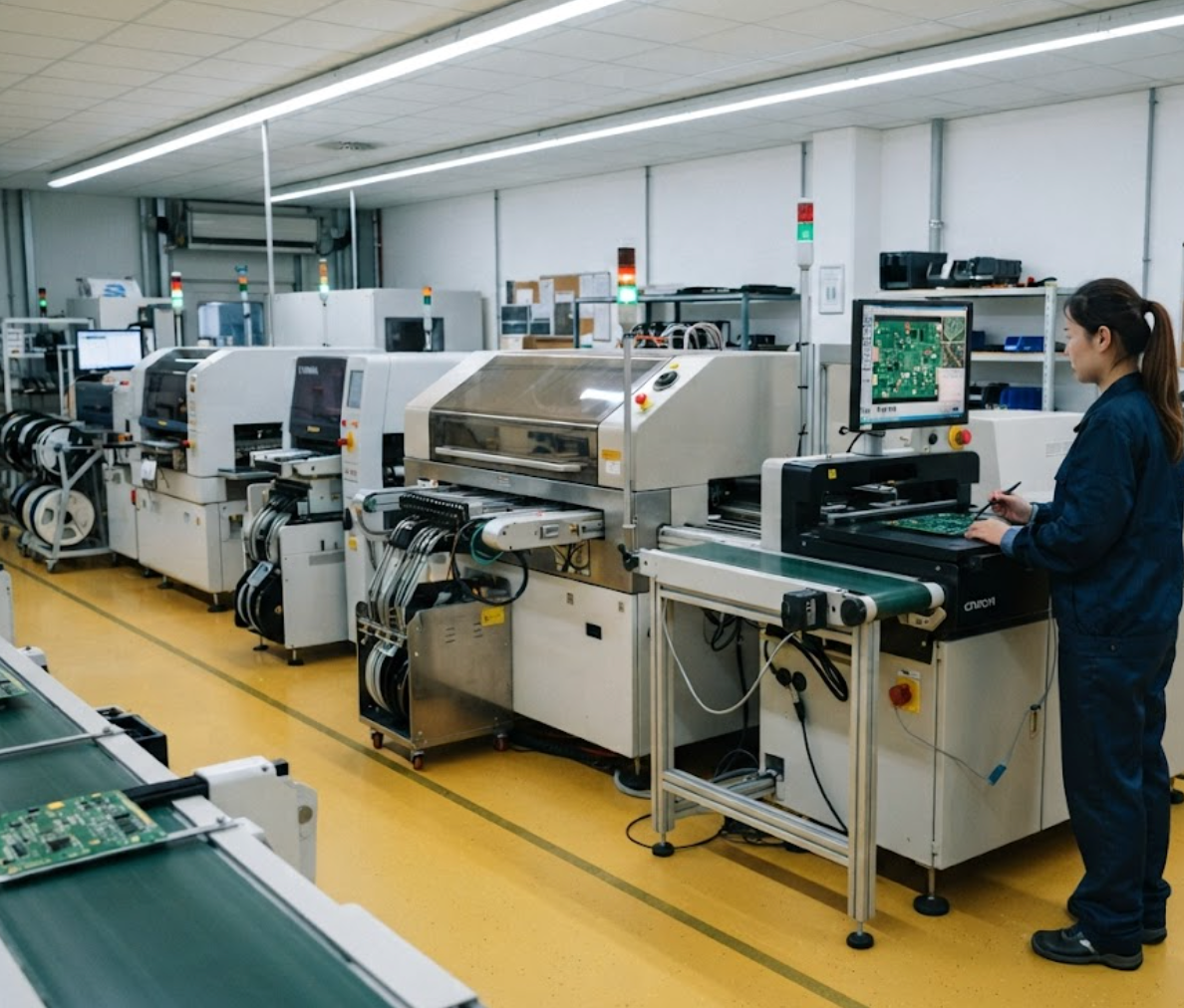
Before we dig into the numbers, here's the foundation: every project we take on—whether it's a dedicated component procurement solution or a full turnkey build—starts with the same question. What does your product need to survive in the real world? Because the answer determines everything from solder paste selection to testing protocols.
Why Yield Rate Data Matters More Than Component Price
Here's what nobody tells you about PCB fabrication and assembly in 2025: component costs have stabilized, but labor and quality-control costs have risen sharply. The global shift toward electric vehicles and IoT devices has created massive demand for high-reliability boards. According to recent industry reports, the automotive electronics sector alone is expected to grow by 8% annually through 2030. That growth brings a problem—smaller batches, faster turnarounds, and zero tolerance for defects. If your contract manufacturer doesn't have real-time data on every solder joint, you're flying blind. The reality is that a low bid on a purchase order often hides the true cost of downstream failures.
At NEWEI, we track over forty quality metrics per batch. But the ones our clients care about most are the first-pass yield (FPY) and the defective parts per million (DPPM). Our current FPY across all SMT Assembly lines stands at 99.7%. We publish this number monthly because it keeps us accountable. When a client's board hits our line, we know exactly where every component came from, which reel it was pulled from, and which operator ran the machine. This level of granularity is not about micromanagement; it is about creating a feedback loop that prevents defects from ever reaching your customers.
Incoming Material Inspection: The First Gate
Most defects don't start on the assembly line—they start at the receiving dock. A batch of capacitors with slightly off-spec ESR values can cause intermittent failures months later. That's why our IQC (Incoming Quality Control) process is so aggressive. We test a statistically significant sample of every reel, every tray, every tube of components. For critical parts like BGA chips or automotive-grade MOSFETs, we go further, running electrical tests before they ever touch a stencil. This is the stage where our component procurement services shine—we source directly from authorized distributors, avoiding the gray market entirely. The data backs it up: our counterfeit detection rate has intercepted over 200 suspect batches in the last two years, saving clients from catastrophic field failures.
One client—a medical device startup—came to us with a board that had been failing at 7% in the field. Their previous assembler couldn't figure out why. We pulled their BOM, ran our IQC, and found that a single resistor value was drifting under temperature stress. The components were genuine, but the supplier had mixed two revision levels in the same reel. That's the kind of subtle issue that only shows up when you test incoming materials with the same rigor as the finished product. It is a classic example of why the cheapest quote is rarely the most cost-effective solution.
SPI and AOI: Catching Defects Before They Compound
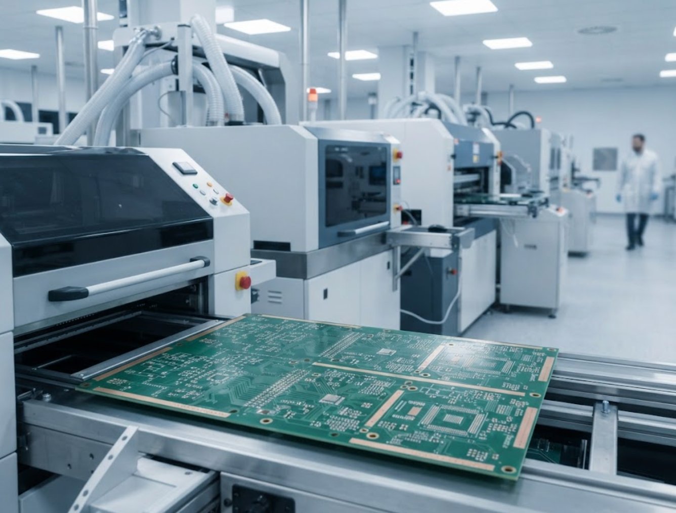
Once materials pass inspection, the real work begins. Our SMT lines run 24/6, placing everything from 0201 micro-components to large BGAs. But placement accuracy means nothing if the solder paste isn't right. That's why every single board goes through Solder Paste Inspection (SPI) before a single component is placed. SPI measures volume, height, and area of the paste deposit. If the paste is too thin, you get cold joints. Too thick, and you risk bridging. Our SPI machines reject anything outside a 5% tolerance window—that's tighter than the IPC-A-610 standard.
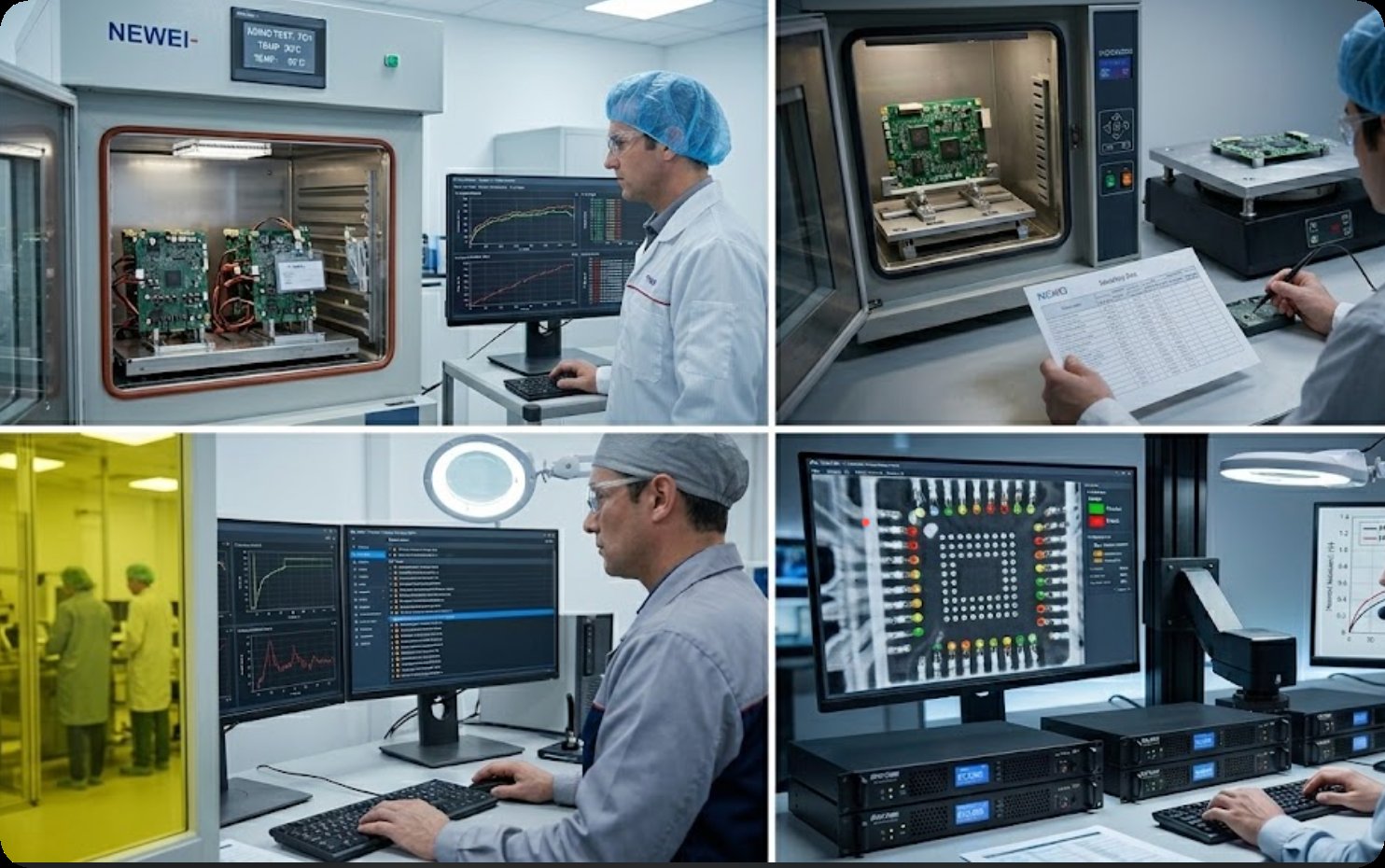
After reflow, each board moves to Automated Optical Inspection (AOI). The AOI checks for missing parts, wrong polarity, lifted leads, and solder defects. It captures images from multiple angles and compares them against a golden board—a reference unit that passed our engineers' manual inspection. Here's a stat that might surprise you: our AOI catches about 97% of all visible defects. The remaining 3% are found by X-Ray inspection, which we use for BGAs, QFNs, and other packages with hidden solder joints. X-Ray gives us a look under the component, verifying that the solder balls have collapsed correctly and formed reliable connections.
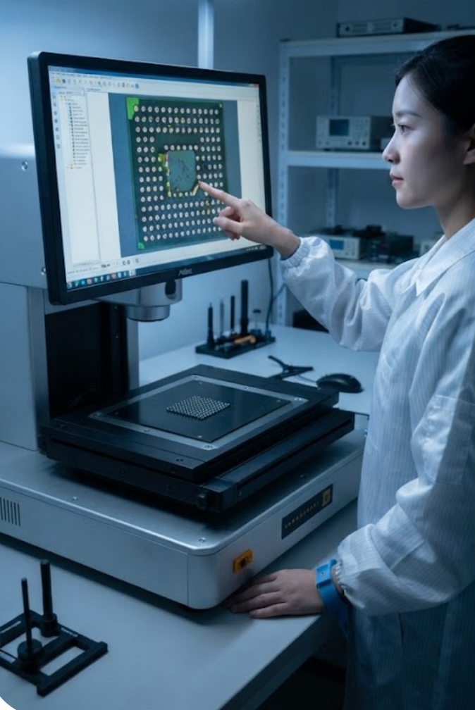
Every board that passes these inspections gets a unique traceability code. If a defect shows up in field testing six months from now, we can trace it back to the exact batch of solder paste, the specific reflow profile, and even the operator who loaded the feeder. That level of traceability isn't just a nice-to-have—it's the backbone of our PCB manufacturing process. It allows us to turn a potential crisis into a data point for continuous improvement.
The Data Behind Our Testing Protocols: ICT, FCT, and Beyond
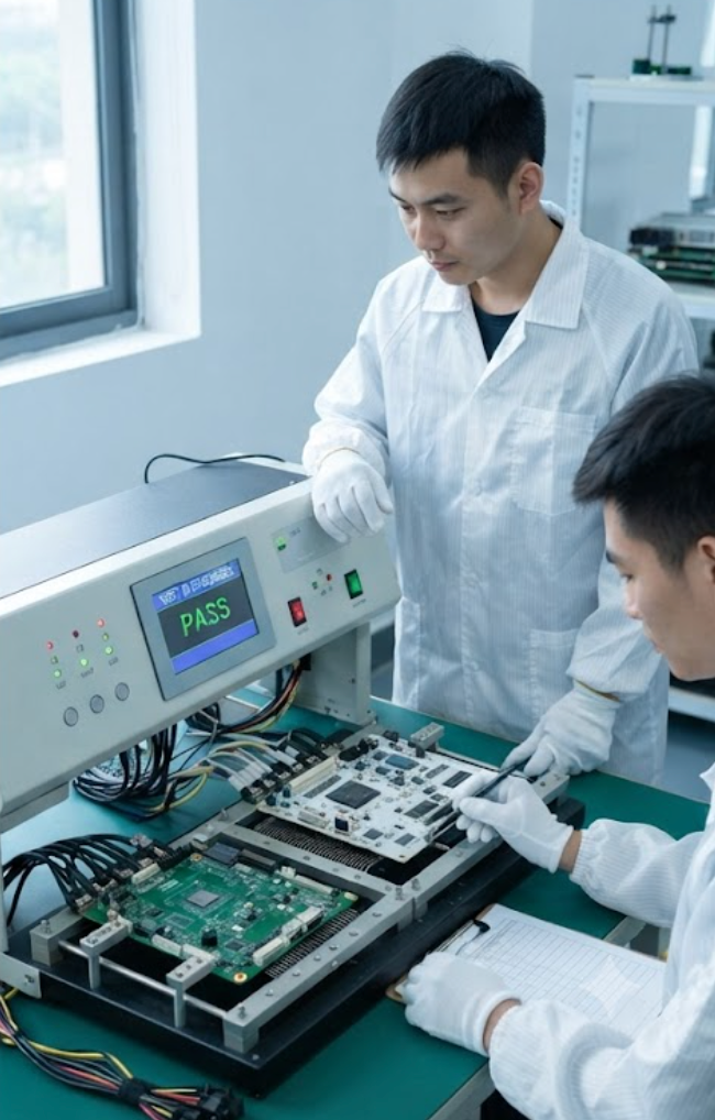
Optical inspection only tells you the board looks right. It doesn't tell you if it works. That's where In-Circuit Testing (ICT) and Functional Circuit Testing (FCT) come in. ICT uses a bed-of-nails fixture to probe every node on the board, checking for shorts, opens, missing components, and incorrect values. It's fast and thorough—a typical board takes about 30 seconds to test. For boards with high component density, we sometimes combine ICT with boundary scan (JTAG) to test digital connections that physical probes can't reach. This is where the theoretical design meets the physical reality of manufacturing tolerances.
FCT goes a step further. It powers up the board and runs it through its actual functions. If you're building a smart thermostat, the FCT fixture will simulate temperature sensor inputs and verify the relay outputs. If you're building an industrial communication board, the FCT will test Ethernet connectivity, serial ports, and GPIO signals. This is where the product-specific knowledge matters. Generic testers can't validate your product's unique features. Our engineers write custom test scripts for each project, ensuring that every function your board is supposed to perform gets verified before shipping. This is not just about checking a box; it is about de-risking your product launch.
The results speak for themselves. In our most recent quarter, we tested over 1.2 million boards across all product lines. The combined failure rate after ICT and FCT was 0.18%. That's a DPPM of 1,800—which is significantly better than the industry average of 5,000 to 10,000 DPPM for mid-tier assemblers. For context, a DPPM of 1,800 means that for every million boards we ship, only 1,800 might have a latent defect. For many of our clients, this is the difference between a routine warranty provision and a financial disaster.
| Metric | NEWEI (2025) | Industry Average |
|---|---|---|
| First-Pass Yield (FPY) | 99.7% | 96%–98% |
| Defective Parts Per Million (DPPM) | 1,800 | 5,000–10,000 |
| Post-ICT/FCT Failure Rate | 0.18% | 1.5%–3% |
| SPI Tolerance Window | ±5% | IPC-A-610 baseline |
| Counterfeit Batch Interceptions (2 yrs) | 200+ | N/A |
Combining Products and Services: A Case Study in Synergy
To show you how these services come together, let's look at a recent project involving two products from our catalog: the OMW-4210A-1L2C2E/LV industrial communication motherboard and a rugged handheld PDA terminal. These are very different boards—the motherboard is a complex, multi-layer design with high-speed differential pairs, while the PDA is a compact, battery-powered device with a touchscreen controller and wireless modules.
Both boards needed SMT assembly, but the PDA also required conformal coating to protect against moisture and dust. The motherboard, on the other hand, needed a more aggressive burn-in test because it's designed for 24/7 operation in industrial environments. Here's how we handled it:
For the industrial motherboard:
Full SMT assembly with SPI and AOI inspection on every board.
X-Ray inspection on the BGA packages to verify solder joint integrity.
ICT to check for shorts and opens across all 1,200 test points.
A 48-hour burn-in test at elevated temperature (60°C) to catch early-life failures.
For the rugged PDA:
SMT assembly with a tighter stencil design to accommodate the 0.4mm pitch components.
Selective conformal coating using our PCBA three-proofing paint services to protect the board without covering the test points.
FCT that simulates GPS lock, Wi-Fi connectivity, and barcode scanning functions.
A drop test on three sample units from each batch to verify mechanical robustness.
By combining these two projects under one roof, the client saved roughly 30% on logistics costs and cut their lead time by two weeks. They also got a single point of contact for quality issues—if something went wrong, they didn't have to argue with multiple vendors about who was at fault. This is the value of a full-service EMS partner. When we handle both industrial PC PCBA and consumer-grade assembly, we can cross-pollinate best practices and apply lessons learned from one product line to another. The result is a more resilient supply chain for you.
Real-World Applications: Where This Level of Quality Matters Most
You don't need 99.7% first-pass yield for every product. But for certain industries, the cost of failure is so high that anything less is unacceptable. Here are the sectors where our clients see the biggest impact from rigorous QC:
Automotive Electronics
Automotive boards face extreme temperature swings, vibration, and electromagnetic interference. A single faulty solder joint in an engine control unit can trigger a recall that costs millions. Our automotive electronics PCBA line uses enhanced inspection protocols, including 100% X-Ray on all BGA packages and a thermal cycle test from -40°C to +125°C on sample units. One client in this space—a manufacturer of EV battery management systems—reduced their field failure rate from 1.2% to 0.05% after switching to our full-service model. That is not just an incremental improvement; it is a step-change in reliability.
Medical Devices
Reliability isn't optional when a board controls a patient monitor or an infusion pump. Medical PCBA requires documented traceability from component lot to finished unit. Our incoming inspection process logs every batch, and our test results are stored for seven years. We recently worked with a wearable health tracker manufacturer on their smart medical motherboard FT-C4435U. The board includes an ECG front-end and a Bluetooth radio—two functions that demand clean analog performance and stable digital connectivity. Our FCT fixture for this board tests both, measuring the ECG signal-to-noise ratio and the Bluetooth packet error rate. This level of detail is non-negotiable when patient safety is on the line.
Industrial Automation and IoT
Factories rely on sensors and controllers that run for years without reboot. The FPA-N10A2E Intel Alder Lake-N motherboard is a prime example—it's designed for edge computing applications where downtime costs thousands of dollars per minute. We put this board through a 72-hour burn-in with a continuous load test, verifying that the CPU doesn't throttle under sustained use and that all I/O ports maintain signal integrity. Clients in this segment appreciate our willingness to share raw test data. We export the full test logs to their quality team, so they can audit our work without having to trust our word. This transparency builds long-term partnerships.
Consumer Electronics and Smart Home
Consumer products face a different kind of pressure: cost. You can't spend $50 testing a device that retails for $89. But you also can't ship a product that fails in the first month. Our balance for consumer electronics is a streamlined testing approach—AOI on every board, ICT on a sampling basis, and FCT on every board that has a microcontroller. We also do drop testing and temperature cycling on a statistical sample. For our smart electric toothbrush PCBA board, we added a waterproof test because the device gets exposed to moisture daily. The board is coated with our conformal coating, then subjected to a simulated splash test before packaging. It is about matching the test intensity to the product's real-world environment.
Market Shifts Reshaping Electronics Manufacturing Services
If there's one trend that defines this year, it's the shift toward smaller, more specialized production runs. The days of ordering 100,000 identical boards are fading. Instead, we're seeing orders for 500 to 5,000 units with multiple variations—different memory sizes, different connectivity options, different enclosure colors. This puts enormous pressure on assembly lines to switch over quickly without sacrificing quality. Our average changeover time is under 15 minutes, which means we can handle mixed-model production efficiently. This agility is not just a convenience; it is a strategic advantage in a market that demands customization.
Another trend is the increasing use of embedded components and HDI (High-Density Interconnect) boards. These boards have micro-vias and buried vias that push the limits of traditional inspection. X-Ray becomes essential, not optional. We've invested in 3D X-Ray systems that can reconstruct the internal structure of a board and detect voids in solder joints with sub-micron accuracy. This technology has been a game-changer for our EMS electronic manufacturing services, allowing us to offer a level of quality control that was previously only available to aerospace and defense companies. We are bringing that aerospace-grade rigor to commercial projects.
Finally, there's the supply chain factor. Component lead times have stabilized, but they're still longer than pre-pandemic levels. Our procurement team actively manages inventory buffers for clients with long production runs, and we offer consignment warehousing for clients who want to lock in component pricing. This is where our dedicated component procurement solutions provide real value—we negotiate pricing, manage aging inventory, and ensure that your boards use components that are current and available, not obsolete parts that will cause headaches in two years. It is about de-risking your supply chain, not just filling a purchase order.
How to Evaluate Your Current PCB Assembly
Tags: SMT assembly / PCB fabrication / PCBA / EMS / NEWEI /
Prev: PCB Fabrication and SMT Assembly Transform Aging Reliability Operations