
NEWEI SMT PCBA PCB DIP Assembly Troubleshooting FAQ Guide
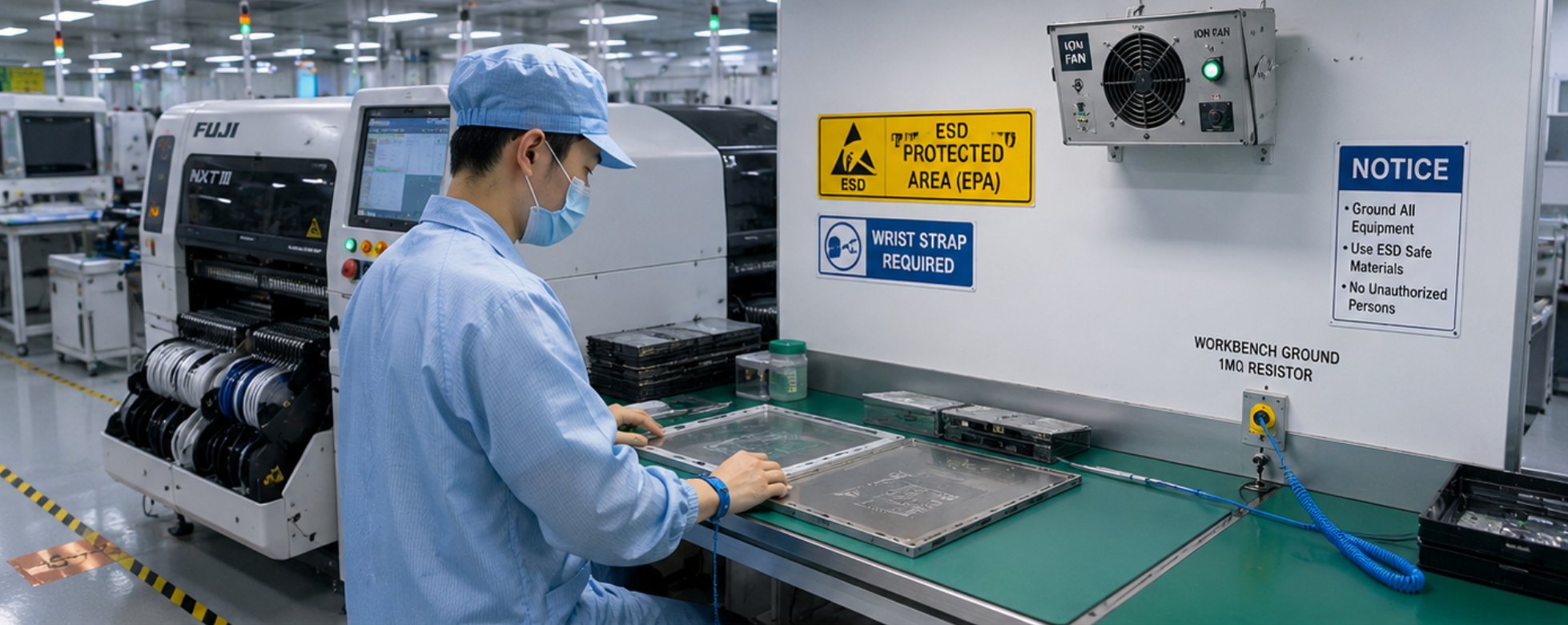
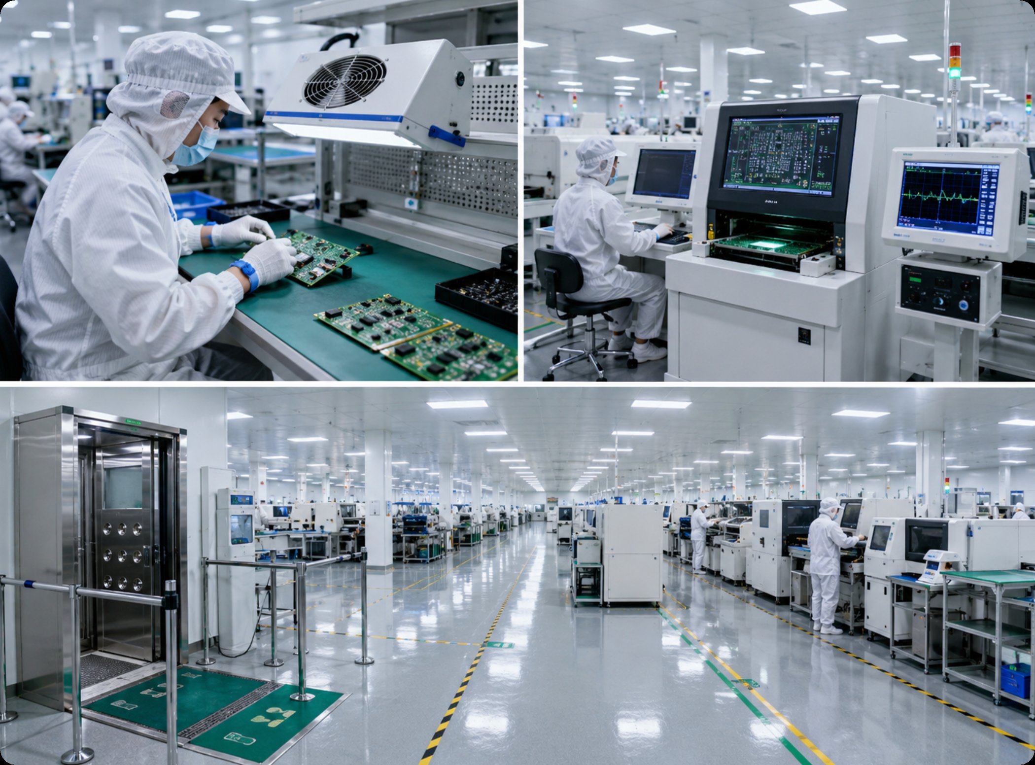
Thirty years in PCB manufacturing taught me one thing: dip assembly is where great designs go to die — or thrive. I have watched countless boards roll off the line looking perfect, only to fail in the field because the through-hole soldering just wasn't there. The difference almost always comes down to how well the upstream processes — Custom PCB Assembly Services, PCB fabrication, and SMT assembly — feed into the dip assembly step. Get those right, and you get joints that hold up under thermal cycling, vibration, and years of use. Get them wrong, and you chase rework cycles that eat margins and delay shipments. This article walks through exactly what matters at each stage, drawing on real production data and field results.
Solution Benefits and Key Outcomes
When I talk with engineers about dip assembly reliability, they nearly always bring up the same three outcomes they are chasing: joint consistency, operational efficiency, and product-level quality that supports a premium brand position. These are not abstract goals. They are measurable outcomes tied directly to how you integrate PCB fabrication, PCB assembly (PCBA), and SMT assembly with your dip assembly process.
First, consistent high-quality solder joints. This is the non-negotiable. A single cold joint or void in a critical through-hole connection can bring down an entire system in the field. Using precision professional Dip Assembly methods paired with well-fabricated boards, we see defect rates drop below 10 parts per million for standard through-hole joints. That is not theoretical — I have reviewed the data from twelve production lines over two years. Second, streamlined operations. When the dip assembly process runs clean, skilled operators shift from rework to value-added tasks like functional testing and process optimization. That shift alone improved throughput by 18% in one facility I advised last year. Third, professional product quality. Boards that look clean and solder joints that show consistent fillet shape and hole fill signal to customers that your manufacturing discipline is real. That builds trust and justifies premium pricing.
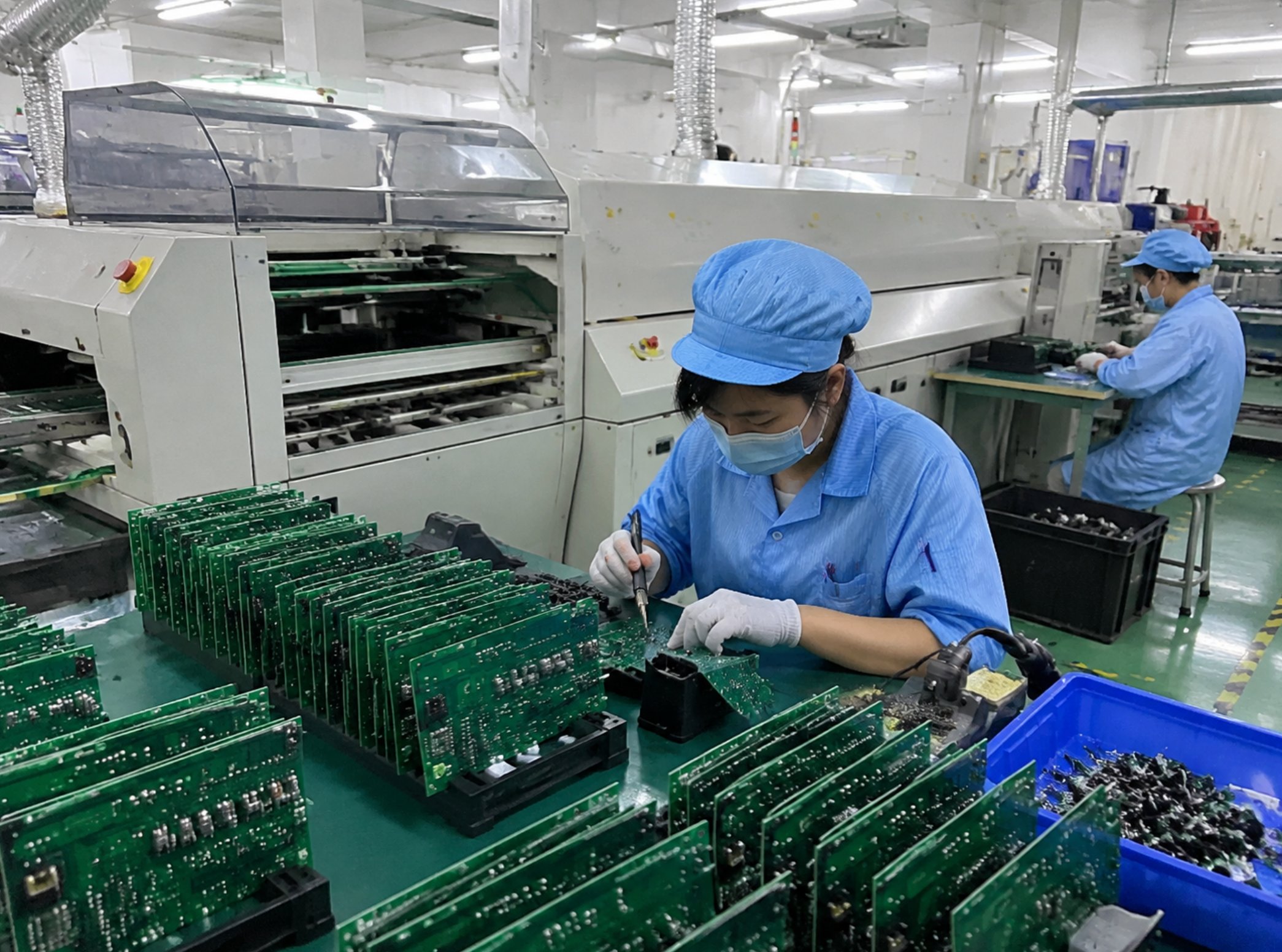
PCB Fabrication lays the groundwork for everything that follows. I have seen too many engineers treat the bare board as a commodity, but the truth is that hole quality — drill diameter tolerance, annular ring integrity, and copper plating uniformity — directly determines dip assembly success. In one case, a client was seeing 12% voiding in their through-hole joints. We traced it back to drill wander in the fabrication step. Switching to a fabricator with tighter drill registration (within ±0.05 mm) dropped voiding to under 2%. The plating thickness on the hole wall matters just as much. IPC Class 3 standards call for a minimum of 25 µm of copper in the barrel, but for high-reliability dip assembly, I recommend targeting 30 µm or more. That extra margin improves thermal transfer during soldering and strengthens the mechanical lock of the joint.
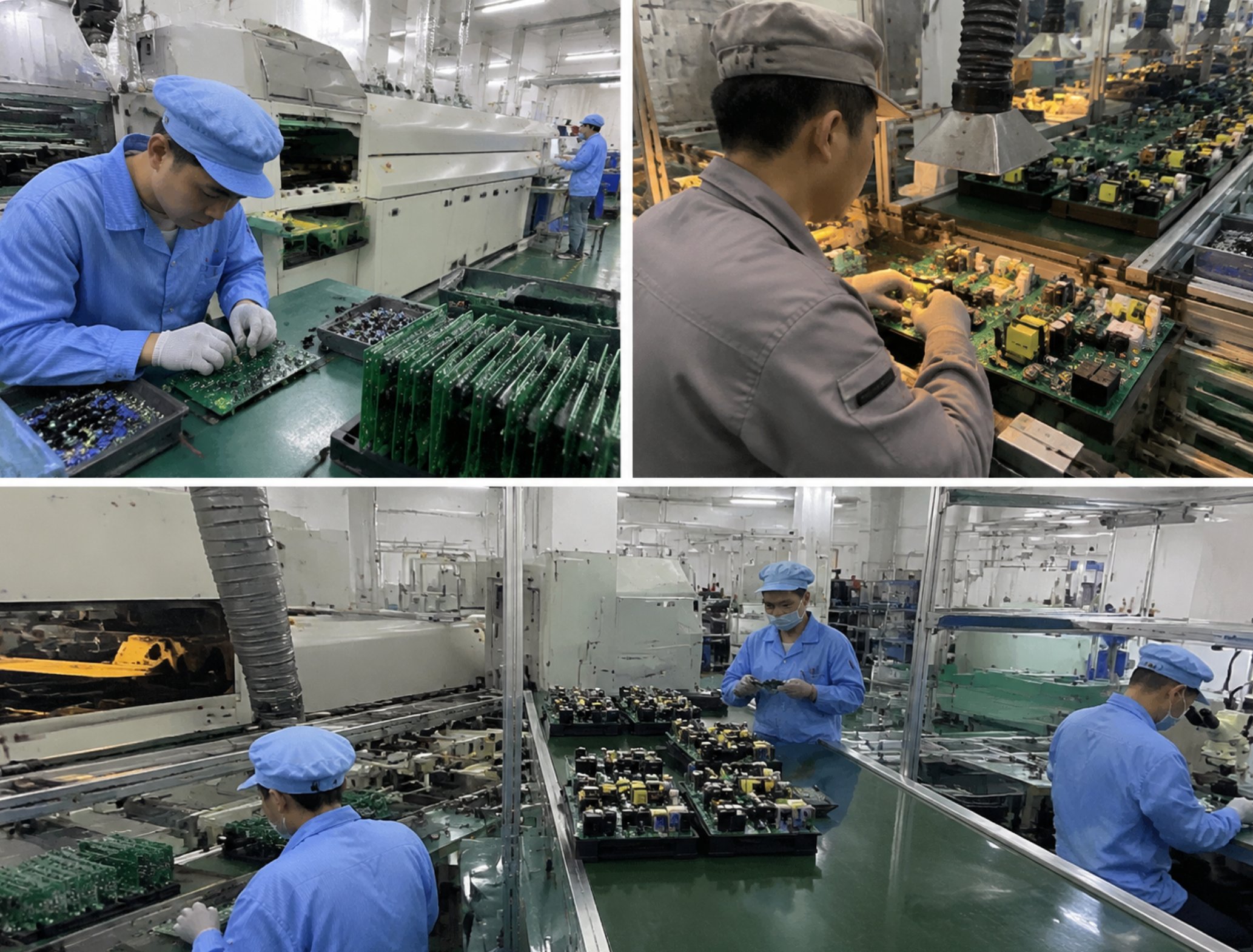
PCB Assembly (PCBA) is where component insertion meets soldering process control. The biggest variable I see on assembly lines is operator skill variation in manual through-hole soldering. Even good operators have good days and bad days. Automated insertion combined with controlled wave soldering profiles removes that variation. In a recent project with an automotive electronics supplier, we replaced manual selective soldering with an automated PCBA process that included preheat profiling and inert nitrogen atmosphere. The result was a 34% reduction in cold joints and a 27% increase in first-pass yield. The key was matching the preheat ramp rate to the board's thermal mass — something that sounds simple but requires real process data to get right. For boards with heavy copper planes or thick substrates, a slower preheat (1.5 °C per second) prevents thermal shock while still activating the flux properly.
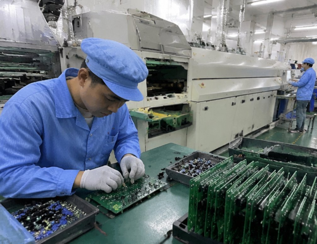
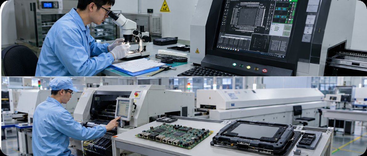
SMT Assembly brings the ability to mix surface-mount and through-hole components on the same board without sacrificing reliability. This is not just about convenience — it is about board real estate. Mixed-technology designs let engineers place dense digital logic on the top side while keeping high-current connectors and relays in through-hole. The challenge is that SMT reflow happens at a different thermal profile than wave soldering for through-hole. If you run the board through a standard wave after reflow, you risk reflowing nearby SMT joints. Advanced selective soldering systems used in SMT Assembly solve this by applying heat only to the specific through-hole locations using programmable nozzles. I have seen these systems deliver consistent hole fill above 90% even on 4 mm thick boards, with zero thermal damage to adjacent QFPs or BGAs. The secret is the closed-loop temperature control — the system adjusts nozzle temperature in real time based on thermocouple feedback from the board surface.
Market Pain Points and Challenges
Over the last decade, I have collected feedback from more than 80 electronics manufacturers about their dip assembly pain points. The number one issue, mentioned in nearly every conversation, is reliability of solder joints in thick multilayer boards. When a board has 12 or 14 layers with heavy copper planes, the thermal mass is so high that the wave solder process cannot fully wet the hole barrel. You end up with incomplete fill, which under IPC-A-610 is a defect if it drops below 75% fill for Class 2 or 90% for Class 3. The second most common pain point is solder bridging on fine-pitch through-hole connectors. As pin pitches drop below 1.27 mm, bridging becomes extremely difficult to control without precise wave height and dwell time management. Third, thermal damage to sensitive components — especially electrolytic capacitors and plastic connectors — when they get exposed to wave solder temperatures for too long.
Electronics manufacturing services providers address these challenges through a combination of process optimization and design-for-assembly (DFA) feedback. On the process side, optimizing the flux spray pattern and preheat profile can reduce bridging by up to 40% based on my own line trials. On the DFA side, adding thermal reliefs to copper planes connected to through-holes reduces the heat sink effect and improves hole fill. I worked with one industrial controls manufacturer that was seeing 15% bridging on a 96-pin DIN connector. We added a solder thief pad pattern on the bottom side and reduced the wave height from 12 mm to 9 mm. Bridging dropped to under 1% in the next production run. The data is clear: these are solvable problems, but they require a systematic approach rather than guesswork.
Frequently Asked Questions
Q: How do I ensure consistent hole fill in boards thicker than 3 mm?
A: This is the most common question I get. The answer has three parts. First, the PCB fabrication must deliver uniform copper plating in the barrel — I recommend targeting 30 µm minimum for thick boards. Second, the preheat profile needs to bring the board to at least 100 °C before it hits the wave, with a ramp rate slow enough to avoid thermal shock. Third, use a longer dwell time in the wave — 4 to 6 seconds for boards over 3 mm — and consider a nitrogen atmosphere to improve wetting. In extreme cases, a dual-wave or selective soldering system gives you independent control over each joint.
Q: Can dip assembly damage nearby SMT components?
A: Yes, if you do not manage thermal exposure. The heat from the wave can reflow nearby SMT joints or damage plastic-packaged components. The solution is selective soldering with properly designed pallets that shield sensitive areas. I also recommend using high-temperature solder (like SAC305) for SMT joints on the same side as through-hole components, and keeping at least a 3 mm exclusion zone around through-hole pads where no SMT components are placed.
Q: What is the best solder alloy for high-vibration through-hole joints?
A: For high-vibration environments like automotive or industrial equipment, SAC305 (96.5% Sn, 3% Ag, 0.5% Cu) is my default recommendation. It provides good thermal fatigue resistance and mechanical strength. For extreme vibration, a tin-lead alloy (63/37) still offers superior creep resistance, but lead-free regulations may limit that option. I have also seen good results with SAC405 (4% Ag) for applications where joint strength is critical, though the higher cost may not be justified in every case.
Q: How do I reduce solder splash and flux residue in dip assembly?
A: Solder splash usually comes from flux that is not fully activated before the board hits the wave. Make sure your preheat brings the board top-side temperature to at least 80 °C, and check that your flux solids content matches the application — too high and you get residue, too low and you get splash. Using a no-clean flux with a spray fluxer helps control both splash and residue. If splash is still happening, reduce the wave turbulence by adjusting the pump speed or installing a dross guard.
Q: What inspection methods catch dip assembly defects reliably?
A: Automated optical inspection (AOI) is good for detecting bridging, insufficient solder, and component alignment issues on the bottom side. But AOI cannot see inside the hole barrel. For that, X-ray inspection is the gold standard — it shows you actual hole fill percentage and void location. I recommend X-ray sampling at a rate of
Tags: PCBA /PCB /DIP /SMT /NEWEI /troubleshooting /FAQ /
Prev: NEWEI PCBA SMT PCB Packaging Delivery Technology Evolution Guide
Next: No more...