
Advanced SMT Assembly Techniques for High-Reliability Industrial Motherboards
Advanced SMT Assembly Techniques for High-Reliability Industrial Motherboards
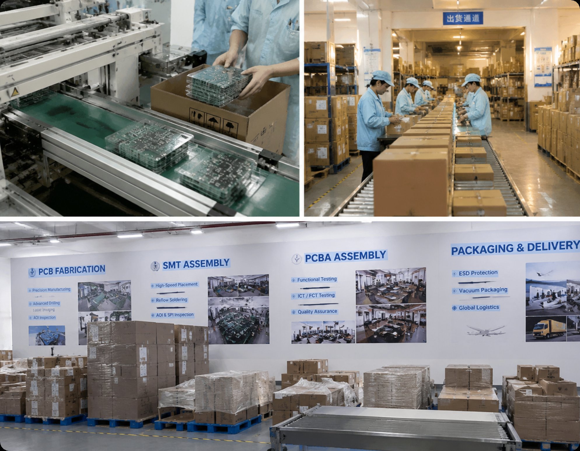
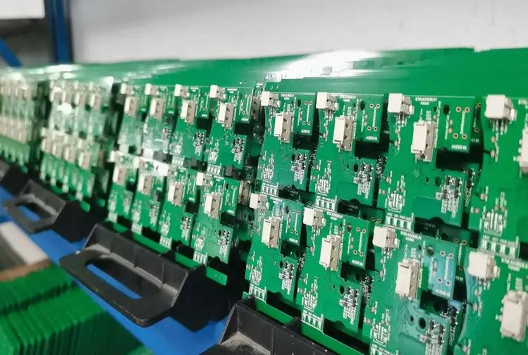
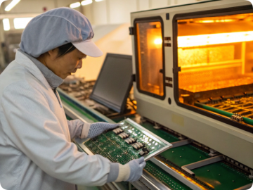
Industrial motherboards demand a level of robustness that far exceeds consumer-grade electronics. Operating in harsh environments—from factory floors with vibration and dust to outdoor telecom stations with extreme temperature swings—these boards require specialized PCBA manufacturing processes. Unlike standard PCBs, industrial motherboards often use thicker copper layers (2 oz to 4 oz or more) to handle higher currents and improve thermal dissipation. The assembly process must account for these heavier substrates, which require precise temperature profiling during reflow to avoid delamination or incomplete solder joints. At Custom PCB Assembly Services, we tailor every SMT line parameter to the specific copper weight and board thickness, ensuring reliable solder connections from the first component to the last.
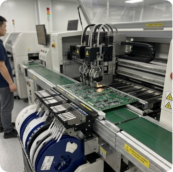
The foundation of any high-reliability industrial motherboard is its SMT assembly process. Advanced pick-and-place machines with high-speed placement accuracy (±25µm or better) are essential for fine-pitch components like BGAs and QFPs. For industrial designs, we see frequent use of 0.5mm pitch BGAs and even 0.4mm pitch for memory controllers. Stencil design becomes critical—laser-cut stainless steel stencils with electropolished apertures ensure consistent solder paste volume. We follow IPC-7525 for stencil design, with area ratios above 0.66 to prevent solder balls and bridging. Pre-reflow inspection using 3D SPI (solder paste inspection) catches volume anomalies before components are placed, reducing rework on expensive multi-layer boards. Engineers who have worked with standard prototypes often underestimate the thermal mass of a 4oz copper board; we compensate with a longer soak zone and a controlled ramp rate of 1.5°C per second, which minimizes tombstoning and void formation.
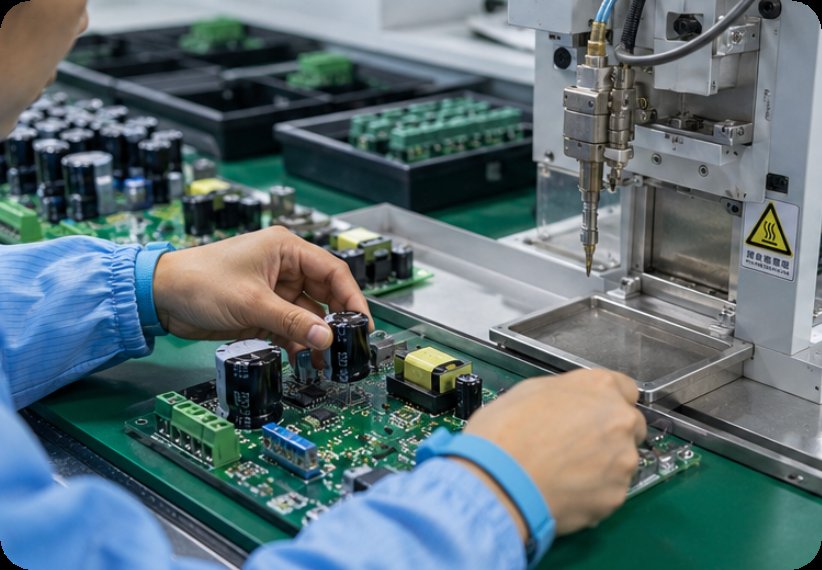
Another factor that separates average assemblies from mission-critical builds is the handling of large-format panels. Industrial motherboards often exceed 500mm in length. Our SMT assembly lines use edge-hold conveyors with adjustable support pins to prevent board sag during reflow. This eliminates stress-induced warpage, which can crack ceramic capacitors or misalign fine-pitch connectors. For mixed-technology boards that combine through-hole connectors with dense SMT, we employ selective soldering robots after the SMT phase. This approach preserves the thermal profile for the surface mount side while delivering reliable fillets on heavy-duty terminal blocks and RJ45 jacks.
BGA Assembly and X-Ray Inspection for Mission-Critical Boards
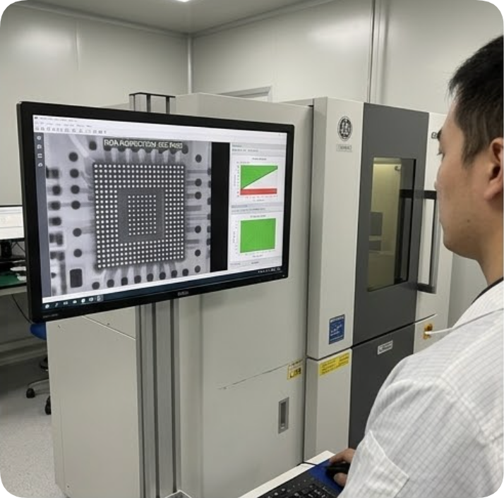
BGA components are the backbone of modern industrial motherboards—they house CPUs, chipsets, and memory controllers. BGA assembly requires strict process control: nitrogen reflow atmosphere reduces oxidation, and ramp-soak-spike (RSS) profiles with a peak temperature of 240–245°C (for lead-free SAC305) ensure full alloy melting without thermal shock. After reflow, industrial PCB reliability hinges on X-Ray inspection of BGA solder joints. Voiding must be kept below 25% per IPC-A-610 Class 3, with no large voids near the joint edge. We use automated X-Ray systems with 0.1µm resolution to detect head-in-pillow defects, non-wetting, and micro-cracks. For critical high-power BGAs on industrial motherboards, we also perform cross-sectioning during first article inspection to validate intermetallic compound thickness (1–5µm ideal).
Beyond BGA inspection, AOI (Automated Optical Inspection) is deployed after reflow for all visible components. However, on industrial motherboards with dense component placement, shadowing can mask hidden joints. That's why we combine AOI with ICT (In-Circuit Test) for analog and digital measurement. ICT fixtures with pneumatic probes access test points on both sides of the board—essential for double-sided SMT assemblies common in industrial designs. Test coverage typically exceeds 90%, checking resistor values, capacitor capacitance, diode drops, and IC power-on sequences. For boards with high-layer counts (12–20 layers), flying probe testers supplement ICT to handle fine-pitch nodes without custom fixtures. In one recent project for a railway signaling system, we reduced false call rates by 40% by programming a custom boundary-scan test for JTAG chains, catching a marginal BGA solder ball that AOI had missed due to under-fill shadowing.
We also emphasize the importance of thermal management during test. High-power industrial boards can draw 50A or more during full load. Our ICT systems incorporate forced air cooling and current-limited power supplies to prevent thermal runaway on the test fixture. This is particularly relevant when testing boards with embedded processors that dynamically adjust clock speeds based on temperature. By maintaining a stable 25°C ambient in the test bay, we get repeatable measurements that correlate with final system performance.
Conformal Coating: Protecting Industrial Motherboards from Environmental Stress
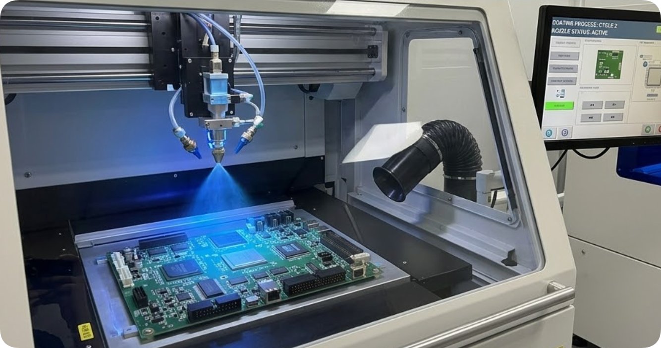
Once electrical testing passes, the next critical step for industrial motherboard PCBA manufacturing is conformal coating. Industrial environments expose boards to humidity, salt spray, dust, and chemical vapors. SMT Assembly Services at NEWEI include selective conformal coating using automated spray robots with precision nozzles. We apply acrylic (AR), silicone (SR), or polyurethane (UR) coatings in controlled thicknesses of 30–150µm, depending on the protection level. Silicone coatings offer the widest temperature range (-55°C to +200°C), ideal for motherboards in kiln controls or refrigeration units. Masking is automated using programmable jetting to protect connectors, test points, and heat sinks. Post-cure inspection under UV light (for UV-cure formulations) or thickness measurement via eddy current sensors ensures uniform coverage. Conformal Coating / Three-Proofing Services are particularly vital for industrial motherboards deployed in outdoor telecom or automotive applications.
Choosing the right coating material involves trade-offs. Acrylic coatings are easy to rework and provide good moisture resistance, but they soften above 100°C. Polyurethane offers better chemical resistance but requires longer cure times. For boards that see thermal cycling from -40°C to +125°C, we recommend silicone with a high elongation rate (over 100%) to avoid cracking. We also apply a secondary underfill on large BGAs before coating to prevent capillary wicking of the conformal coating into the solder joints. This two-step process—underfill followed by selective coating—extends the lifetime of the motherboard in high-vibration environments like mining equipment or wind turbines.
Personal view: In my 12 years of industrial PCB assembly, I've seen too many field failures caused by incomplete coating coverage under tall components. Always use a robotic dispenser with a 3D vision system to map component heights before programming the coating path. Skipping this step can lead to capillary creep that shorts high-voltage pins. A 5-minute pre-scan saves weeks of warranty returns.
Rigorous Testing: ICT, FCT, and Burn-In for Zero-Defect Delivery
After coating, we perform Functional Circuit Test (FCT) on every industrial motherboard. FCT simulates real-world operation—powering up the board, loading firmware, checking voltage rails, clock signals, and communication interfaces (CAN, RS-485, Ethernet). Test programs are custom-developed for each OEM design, often running for 30–60 minutes per board. This is followed by burn-in or aging tests at elevated temperatures (typically 60–85°C) for 24–72 hours. Thermal cycling during burn-in reveals latent defects like cracked solder joints or weak intermetallic bonds. For high-reliability military or medical-grade motherboards, we extend burn-in to 168 hours with voltage margining. All test data is logged per board serial number, providing full traceability back to the SMT line, component lot, and operator.
We also integrate boundary-scan (JTAG) testing into the FCT phase for boards with complex FPGAs or SoCs. This allows us to verify interconnects between BGAs without physical probing. In one production run of 5000 boards for a medical imaging system, boundary-scan caught a 0.3% failure rate in a 0.4mm pitch BGA that had intermittent opens after thermal stress. Without this test, the failures would have only appeared after the customer's system burn-in, costing 10x more to replace. Our test engineers also monitor inrush current during FCT—a sudden spike above 20% of nominal can indicate a shorted decoupling capacitor, which we then isolate with thermal imaging to pinpoint the exact component.
Why Choose NEWEI for Industrial Motherboard Assembly
NEWEI's experience spans over 15 years in industrial motherboard assembly, serving OEMs in automation, energy, medical, and transportation sectors. Our factory is ISO 9001:2015 certified, with dedicated SMT lines for heavy copper boards and mixed-technology assemblies (through-hole + SMT). We maintain strict ESD control (Class 2, <100V) and operate a Class 10K cleanroom for conformal coating. Every order—from prototype runs of 10 boards to volume production of 10,000+—receives the same attention to IPC Class 3 standards. Our engineering team provides DFM feedback before production, optimizing pad designs and thermal reliefs for your specific copper weight and component selection. Contact us to discuss your next industrial motherboard project—from design for manufacturability through full turnkey PCBA manufacturing.
Beyond standard services, we offer design-for-test (DFT) reviews that can reduce your test cycle time by 30%. For example, by adding a few test points on inner layers and using via-in-pad for BGAs, we enable ICT access without compromising signal integrity. Our supply chain team also sources high-temperature-rated components (125°C or 150°C) for the most demanding applications. If you are developing a motherboard for a solar inverter or a railway signaling controller, we can recommend specific capacitor dielectric materials (C0G/NP0 for timing circuits) and connector plating (gold over nickel for corrosion resistance). This level of detail is what sets our PCBA manufacturing apart from generic assemblers.
Optimizing the Supply Chain for Hardened Industrial Designs
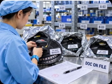
Sourcing components for industrial-grade systems requires an entirely different methodology compared to commercial electronics. Component longevity is paramount; while consumer devices operate on a 2-to-3-year lifecycle, industrial control units, power grids, and railway signaling arrays regularly remain active for 10 to 15 years. At NEWEI, our procurement protocols are built explicitly to eliminate the risks of component obsolescence and counterfeit integration.
- Authorized Franchised Distribution Only: We enforce an unyielding policy of sourcing critical semiconductors, memory ICs, and power modules exclusively through direct manufacturers or tier-one authorized franchised distributors.
- Strict Lifecycle Forecasting (EOL & PCN Tracking): Before committing to a bill of materials (BOM), our engineers cross-reference every part number against global obsolescence databases. We generate lifecycle projections to ensure no critical microcontroller or driver IC is slated for End-of-Life (EOL) within your operational roadmap.
- Alternative Cross-Matching: For long-term production contracts, we identify and qualify drop-in functional alternatives for high-risk passives and discrete semiconductors during the initial design-for-manufacturability (DFM) phase.
When you partner with NEWEI, you are not just hiring an assembly line; you are leveraging an advanced technical supply infrastructure designed to protect your product lifecycle and guarantee continuous operation in the field. For comprehensive engineering verification and manufacturing support, explore our core Custom PCB Assembly Services and discover how we can elevate your product hardware architecture.
Tags: PCBA Manufacturing /Industrial Motherboard /
Prev: Why Your Handheld PDA OEM Partner Must Master Packaging, Testing & Global Delivery
Next: Why Component Quality Control and Supplier Management Make or Break Your PCB Assembly Project