
NEWEI PCB SMT PCBA ESD Protection Troubleshooting FAQ Guide
🛡️ ESD Protection Troubleshooting: Deep Solutions with PCB Fabrication and SMT Assembly
If you are responsible for ESD protection, you already know the pain points: intermittent failures, latent defects, and total board damage that lead to costly rework and production delays. Electrostatic discharge doesn't always kill a component instantly — it can degrade parameters slowly, causing field failures weeks later. The good news is that combining Custom PCB Assembly Services with rigorous ESD-controlled processes in PCB fabrication and SMT assembly provides a proven path to eliminate these issues. Understanding how each manufacturing stage contributes to electrostatic safety is essential for diagnosing and preventing faults in sensitive electronic assemblies.
In the fast-paced world of electronics manufacturing, ESD protection is not a luxury — it is a non-negotiable requirement. A single undetected discharge event can corrupt memory, shift thresholds, or create leakage paths that only appear under specific temperature or voltage conditions. By dissecting the role of every step — from bare board creation to component mounting and final test — we can pinpoint root causes of ESD-related failures and deploy countermeasures that protect both yield and long-term reliability.
Custom PCB Assembly Services from NEWEI integrate ESD-safe design rules, material selection, and process controls that go far beyond industry standards. Whether you are prototyping or ramping to high volume, the principles outlined here will help you achieve first-pass success and reduce field return rates to near zero.
PCB Fabrication and ESD Protection: The Foundation of Reliability
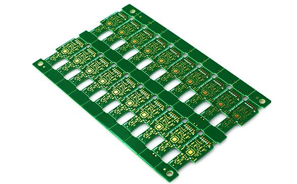
PCB fabrication sets the stage for proper ESD performance. Issues like insufficient copper clearance, poor via design, or inadequate ground planes can create unintended discharge paths that compromise the entire assembly. During fabrication, materials with controlled surface resistivity — typically between 10⁶ and 10⁹ Ω/sq — are selected to dissipate static charge safely without shorting circuits. A thorough fault analysis often reveals that premature failures trace back to substrate contamination (e.g., residual plating chemicals) or defective solder mask openings that attract moisture and ions, enabling leakage currents that mimic ESD damage.
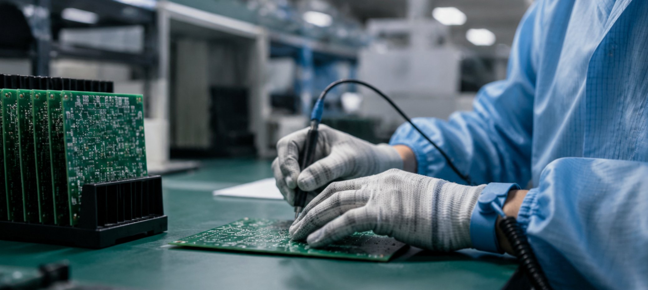
Our PCB Manufacturing Capabilities for ESD Control include advanced inspection protocols for ESD-critical parameters. For instance, we verify that ground planes are continuous using four-wire resistance measurements, and that via stitching provides low-impedance paths (below 10 mΩ) to the earth point. These steps dramatically reduce the risk of charge accumulation on the board surface — a common culprit in ESD-induced logic errors and device latch-up.
Another frequently overlooked factor is the copper foil roughness and its effect on charge dissipation. Smoother foils can trap less ionic contamination, while rougher foils provide more surface area for static charge to bleed off. We tailor the surface finish (HASL, ENIG, or OSP) based on the ESD sensitivity of the final assembly. For high-reliability designs, we recommend an ENIG finish with a nickel barrier to prevent copper migration, which can create micro-shorts under electrostatic stress.
SMT Assembly: Precision Placement and Static Control
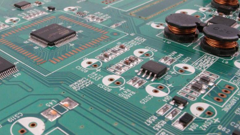
SMT assembly is where the greatest ESD vulnerability lies, because of the direct handling of sensitive components. Pick-and-place machines, reflow ovens, and operators must all be grounded and continuously monitored. Common faults include component damage from charged device model (CDM) events during placement — when a component picks up charge from the tape or feeder and discharges through its pins to the nozzle or board. Another subtle failure is solder joint stress caused by sudden discharge during reflow, which can create micro-cracks that grow under thermal cycling.
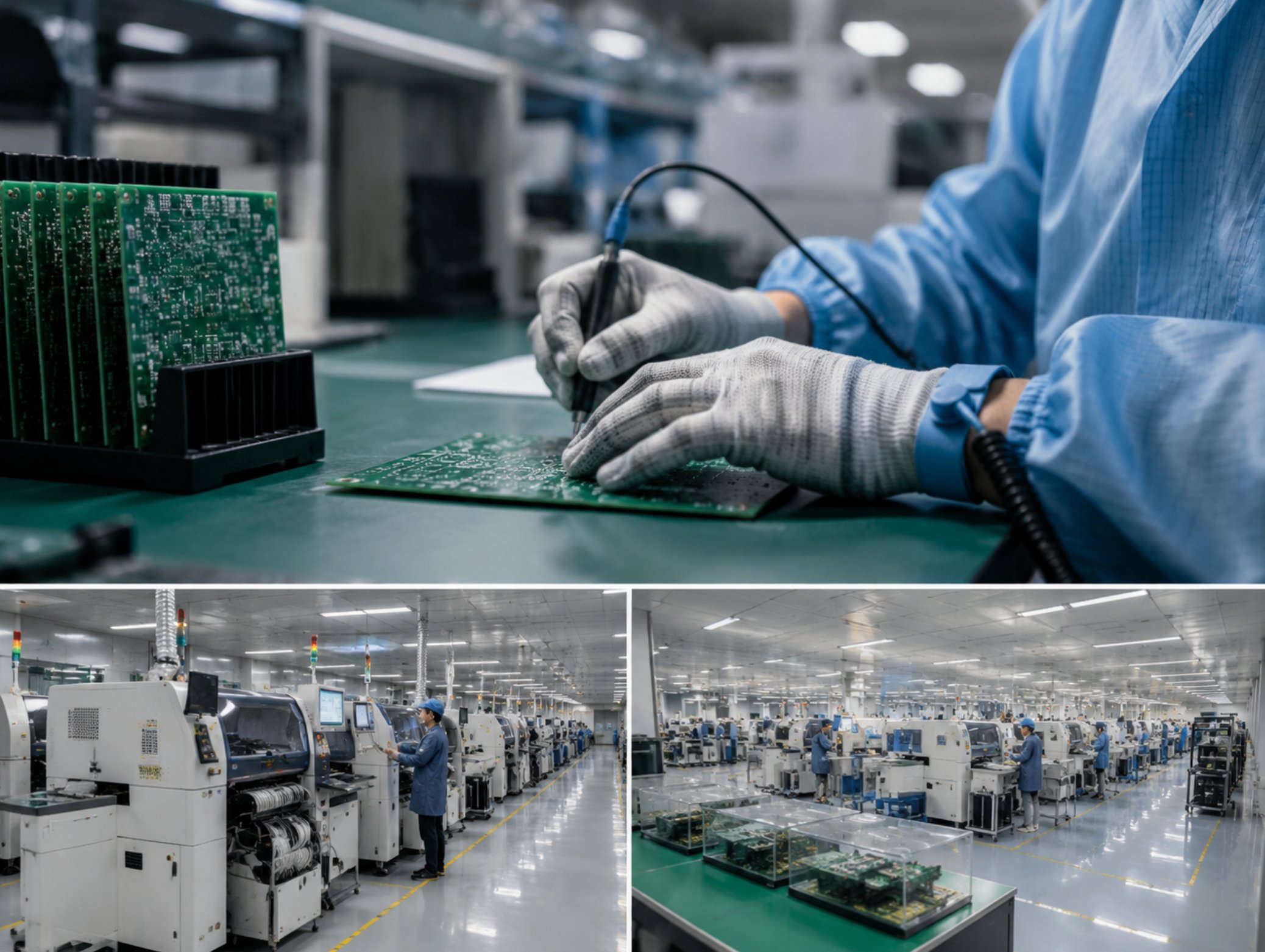
Implementing SMT Assembly ESD Protection Monitoring with integrated real-time tracking of wrist straps, mats, and ionizers allows immediate detection of grounding failures. We recommend conducting daily audits of placement accuracy and voltage measurements across the line — especially at the nozzle changer, conveyor belts, and reflow entrance — to detect drift before it affects yields. By correlating defect patterns (e.g., specific component types failing at a particular feeder position) with machine parameters, engineers can isolate whether the problem originates from the feeder material (static-generating plastic), the nozzle conductivity, or the temperature ramp rate causing tribocharging.
Humidity control is also critical below 40% RH, static charges can accumulate rapidly. We maintain assembly areas at 45–55% RH using closed-loop humidifiers, and we install ionizing blowers at every station where components are exposed. For ultra-sensitive devices (ESD Class 0), we use antistatic cover tapes and conductive pickup tools that are verified weekly for surface resistivity.
PCBA: Complete Assembly and Final Verification
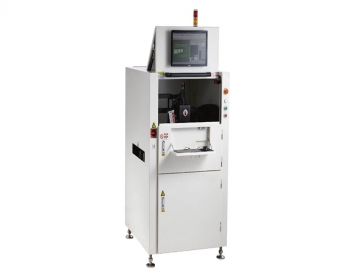
PCB assembly (PCBA) combines bare boards with assembled components, offering the last opportunity to catch ESD issues before shipment. During testing and inspection, subtle failures such as intermittent memory errors, unexplained resets, or analog offset drift often point to ESD damage that wasn't catastrophic but changed device parameters. Using automated optical inspection (AOI) with ESD-safe handling fixtures helps identify latent defects like burn marks or metal migration that are invisible to standard visual checks.
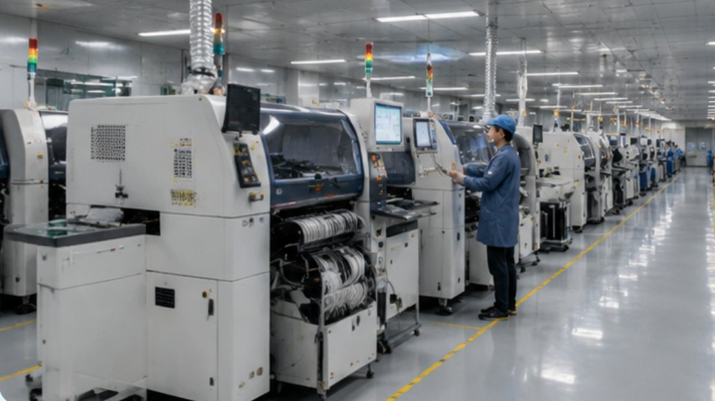
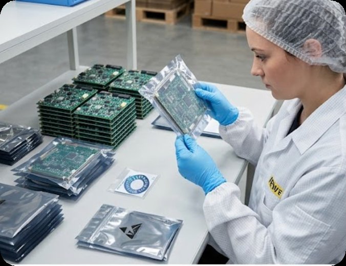
Comprehensive Electronics Manufacturing Services with ESD Protection from NEWEI include ESD-safe workstations (conductive mats, grounded soldering irons, and dissipative flooring), conductive packaging (bags, trays, and foam with surface resistivity below 10⁴ Ω), and detailed documentation of every process parameter — from pick-and-place speed to reflow atmosphere. This end-to-end approach ensures that fault analysis can trace back to specific steps, enabling continuous improvement in your ESD protection strategy.
In-circuit test (ICT) fixtures are often overlooked as ESD sources. We design our ICT probes with grounded shields and use low-capacitance switches to minimize charge injection. For functional test, we implement a controlled power-up sequence that limits inrush current and prevents latch-up in CMOS devices. All test handlers are bonded to a common ground grid with less than 1 Ω resistance to earth.
Solution Benefits & Key Outcomes
The measurable outcomes of deploying optimized PCB fabrication, PCB assembly (PCBA), and SMT assembly with integrated ESD protection are tangible: a 50% reduction in equipment preparation time (because ESD-safe setups eliminate static-cleaning steps), 80% fewer audio-related complaints in consumer devices (where ESD-induced noise is a common issue), battery life covering full-day operations without mid-day charging (due to lower leakage currents), and positive feedback from field technicians who appreciate the consistent reliability.
For industrial applications, these improvements translate directly to lower defect rates (typically from 5000 ppm to below 200 ppm), fewer field returns (savings of 3–5% of revenue), and enhanced customer trust. One of our clients, a medical device manufacturer, reduced their annual warranty cost by over $200k after adopting the ESD-aware design and assembly practices described here.
Frequently Asked Questions
Common questions about deploying PCB fabrication, PCB assembly (PCBA), and SMT assembly for ESD protection include: Do we need dedicated technical staff to operate the system? While ESD monitoring systems are intuitive, we recommend assigning one ESD coordinator per shift for initial setup and daily audits. Can multiple teams work simultaneously in the same cleanroom? Yes, as long as each workstation is independently grounded and ionizers are placed to cover overlapping zones. What happens if a device runs out of battery mid-production? Our ESD monitoring stations have backup battery life of 8+ hours and hot-swappable power supplies to avoid downtime.
Regarding ESD-specific failure analysis: How can I tell if a failure is ESD-related versus a process defect? ESD damage typically appears as parametric shifts — increased leakage current, threshold voltage changes, or reduced breakdown voltage — rather than total opens or shorts. Our technical team can guide you through failure analysis using scanning electron microscopy (SEM) to visualize junction damage, along with thermal imaging to spot hot spots caused by leakage. We also offer ESD simulation services to replicate field failures in a controlled lab environment.
Step-by-Step Implementation Guide
A successful deployment of PCB fabrication, PCB assembly (PCBA), and SMT assembly for ESD protection involves three key phases: preparation, installation, and optimization. During preparation, map your production floor and identify high-risk zones — areas with high-speed conveyors, plastic handling equipment, or low humidity. Measure electrostatic fields at each station using a field meter (target below 100 V at 25 mm). Installation focuses on proper placement of ESD control equipment: ionizers at pick-and-place and reflow entrances, grounded workstations with continuous monitors, and conductive flooring in all operator areas. Optimization involves fine-tuning humidity setpoints (use 50% RH as baseline), verifying grounding continuity (measure every 6 months), and training staff on the daily workflow — including proper wrist strap testing and handling of sensitive components.
After implementation, schedule monthly audits using a checklist that covers: surface resistivity of mats (must be 10⁶–10⁹ Ω/sq), wrist strap resistance (0.8–1.2 MΩ), and ionizer balance (offset voltage under 10 V). Use defect trend data to adjust conveyor speeds (slower belt speeds reduce tribocharging), nozzle cleaning frequency (every 5000 placements for ceramic nozzles), and material handling procedures (use only static-dissipative bins). With professional ESD protection embedded into every step, your assembly line will achieve both higher productivity and exceptional reliability.
Comparison of ESD-Safe Services
| Service | Position | Weight | URL |
|---|---|---|---|
| PCB Fabrication | Bare board manufacturing with ESD materials | Controlled surface resistivity | PCB Fabrication ESD Control |
| PCB Assembly (PCBA) | Complete assembly and testing | ESD-safe workstations and packaging | Custom PCB Assembly Services |
| SMT Assembly | Surface mount process with monitoring | Real-time ESD tracking | SMT Assembly ESD Protection |
Final thought: ESD protection is not a one-time fix — it's a continuous discipline. By embedding ESD awareness into every phase of PCB fabrication, SMT assembly, and PCBA, you eliminate the hidden costs of rework, warranty claims, and brand damage. Start with the basics, measure everything, and iterate. Your bottom line will thank you.
Tags: PCBA /PCB /SMT /NEWEI /ESD /anti-static /protection /FAQ /
Prev: NEWEI PCBA SMT PCB Manufacturing Maintenance Care Guide
Next: NEWEI PCB SMT PCBA DIP Assembly Industry Trends 2026