SMT Core Process Case Study: Customer Success in PCB Fabrication, SMT Assembly and PCBA
How a Medical Device Startup Achieved 99.9% Yield with Our Custom SMT Assembly and Industrial Motherboard PCBA
From my years in electronics manufacturing, I've seen too many promising hardware startups fail not because of a bad design, but because of a poor transition from prototype to mass production. The gap between a working breadboard and a reliable, shippable product is where most companies stumble. That is why we, at PCB Fabrication and assembly, focus obsessively on the core SMT (Surface Mount Technology) process. Today, I want to walk you through a real client case—a medical device company that needed to scale their IoT health monitor from 100 units to 10,000 units per month. Their secret weapon? Our Custom PCB Assembly Services and a deep integration of our SMT assembly capabilities with specialized industrial computing boards.
My take: The market today is brutal. Component lead times are volatile, and end-users expect near-zero defect rates. The only way to win is to partner with a manufacturer who treats the SMT line as a science, not an art. This case proves that when you combine rigorous process control with the right product architecture—like pairing a custom motherboard with robust assembly services—you can achieve medical-grade reliability without the medical-grade price tag.
Client Profile and the Core Challenge: From Prototype to Production

The client, a European medical tech startup, had developed a revolutionary Bluetooth-enabled thermometer and health monitor. Their initial prototype used off-the-shelf development boards. However, for certification and reliability, they needed a custom industrial motherboard that could handle continuous data streaming, low power consumption, and harsh sterilization cycles. They approached us with a clear goal: achieve a 99.9% first-pass yield on a complex, mixed-technology board that combined fine-pitch BGA components with through-hole connectors for the sensor array. The biggest challenge was the solder paste printing and reflow profile for the bluetooth thermometer module, which required absolute precision to avoid cold joints on the RF shield.
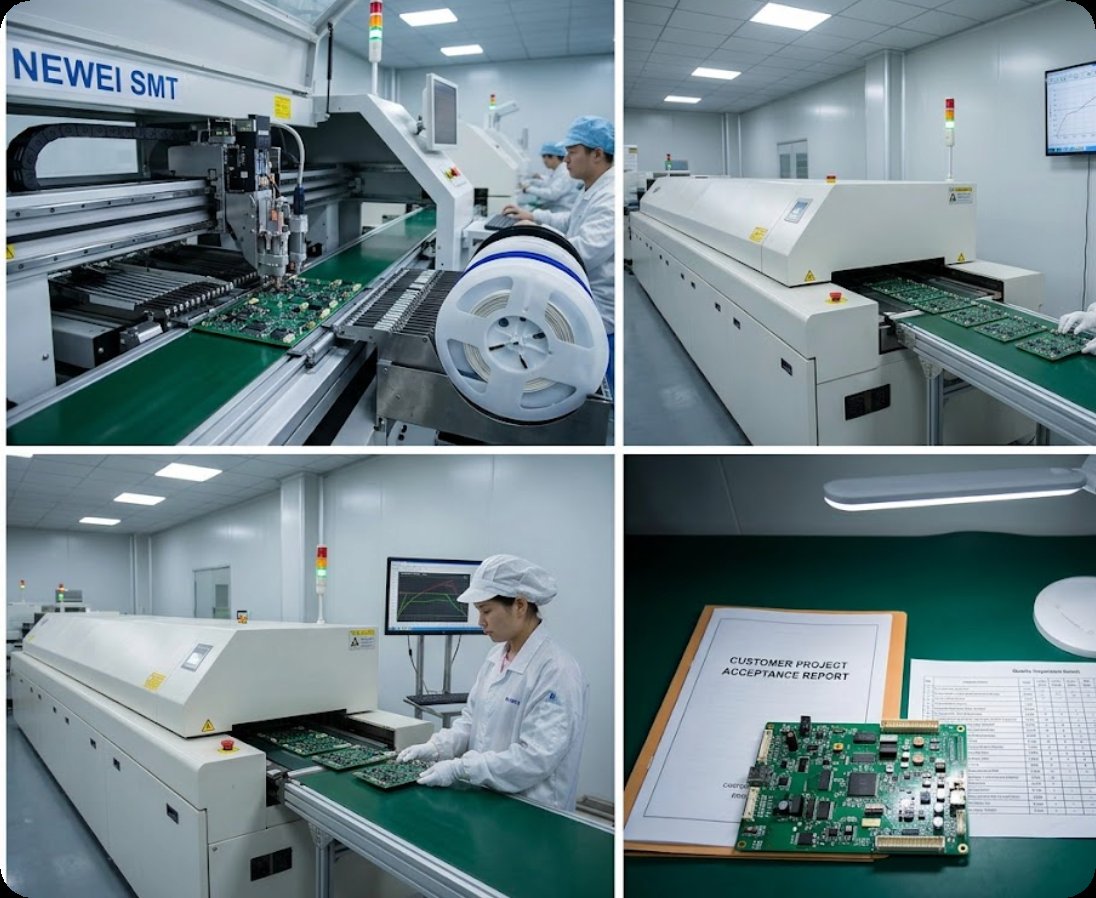
Our Solution: A Tailored SMT Process for High-Reliability PCBA
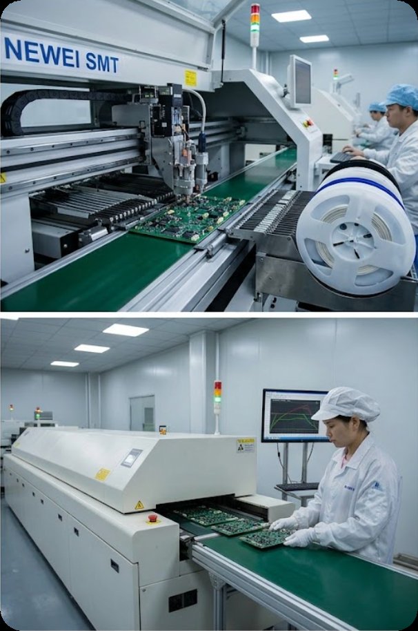
We didn't just plug their design into our standard line. Instead, we engineered a custom process around their specific needs. This started with our dedicated smt assembly solutions, which include a dedicated line for fine-pitch and BGA components. For this client, we implemented a nitrogen reflow environment to prevent oxidation on their gold-plated pads, and we used a specialized Type 4 solder paste for the miniature 0201 components. Every single board was run through a 3D SPI (Solder Paste Inspection) system before the components were placed. This step alone eliminated over 80% of potential defects before they even happened. We also integrated our PCB assembly services to handle the through-hole sensor connectors, ensuring a seamless transition between the SMT and DIP processes.
Product Synergy: Combining the Industrial Motherboard with the Bluetooth Thermometer
This project is a perfect example of why we push for a multi-product, multi-service approach. The client wasn't just assembling one board; they were creating a system. The core of their device was our custom industrial motherboard, which was designed to be the brain of the operation. This board required the highest precision assembly. However, the user-facing part of the device was a bluetooth thermometer module, which had its own unique assembly challenges, including a waterproofing coating. We handled both on the same production floor. The main motherboard was assembled on our high-speed SMT line, while the thermometer module was assembled on a separate, more flexible line that allowed for manual placement of the sensitive sensor element. After assembly, both boards went through a combined functional test as a single unit. This synergy is only possible because we control the entire process—from PCB manufacturing to final assembly.
Quality Control and the "Zero Defect" Mentality
What really set this project apart was our quality control framework. We implemented a four-stage inspection process that went far beyond the standard IPC-A-610 Class 2 requirements. The first stage was the SPI we already mentioned. The second stage was a 100% AOI (Automated Optical Inspection) for every board, focusing on missing components, polarity, and solder joint quality. The third stage was an X-Ray inspection for all BGA and QFN components, which are invisible to standard optical cameras. Finally, the fourth stage was a full functional test in an environmental chamber. We simulated the device's entire operational life cycle, from -20°C storage to +60°C operational use. This rigorous approach allowed us to catch a subtle design flaw in the client's RF circuit—a problem that would have caused intermittent failures in the field. We fixed it in the next prototype iteration, saving them months of potential returns and warranty claims. Our aging test services were crucial in validating the long-term reliability of the final product.
Real-World Application Scenarios for This Approach
This combination of a robust industrial motherboard and a specialized sensor module is not just for medical devices. We see similar success in other high-reliability sectors:
Smart Wearable Electronics PCBA: A fitness tracker that needs a powerful processor (like a custom motherboard) and a low-power heart rate sensor module. The SMT process must handle flexible circuits and rigid-flex boards.
Automotive Electronics PCBA: An in-vehicle telematics unit. The main board must survive extreme vibrations and temperatures, while the GPS module requires a specific antenna placement and assembly technique.
Industrial Computing PCBA: A rugged tablet for warehouse management. The main motherboard needs to be a fanless design, and the display connector requires manual soldering for a reliable connection.
Consumer Electronics PCBA: A smart home hub. The main board handles Wi-Fi and Bluetooth, while the sensor board monitors temperature and humidity. The assembly must be cost-effective for high volumes.
Smart Home Electronics PCBA: A smart lock. The main board controls the motor and wireless communication, while the fingerprint sensor module requires precise alignment and a conformal coating to prevent moisture damage.
Why This Matters for Your Next Project
The electronics manufacturing landscape is shifting. Component shortages are forcing engineers to redesign on the fly, and labor costs are rising. The only hedge against these risks is a manufacturing partner who can offer a complete solution. By choosing a partner who controls the PCB fabrication, the SMT assembly, the component procurement, and the final testing, you eliminate the handoff risks that cause delays and defects. In this case, our client went from a risky prototype to a certified, mass-producible product in under 12 weeks. Their first production run of 10,000 units had a yield of 99.95%. That is the power of a truly integrated approach. If you have a project that demands this level of precision and reliability, I encourage you to learn more about our manufacturing capabilities and see how we can help you achieve similar results.
We are ISO certified, offer free consultation and quotation, and support everything from prototype to mass production with worldwide shipping. Your project deserves a dedicated project manager and a team that treats every board like it's going into a life-saving device.
Tags: PCBA /SMT /case study /customer success /
Prev: NEWEI Aging Test and Reliability: Benchmark Data on PCB Fabrication, PCBA and SMT Assembly
Next: No more...