Navigating the Technology Evolution in SMT Core Processes for Modern Electronics Manufacturing
Navigating the Technology Evolution in SMT Core Processes for Modern Electronics Manufacturing
Over the past decade, I have watched the PCB assembly industry shift from manual through-hole assembly to fully automated surface-mount lines that operate at astonishing speeds. The real challenge today isn't just placing components—it's maintaining precision across increasingly miniaturized designs while keeping cost and lead time under control. In my experience, partnering with a proven Custom PCB Assembly Services provider becomes the single most important decision in your production cycle, especially when your product relies on the latest SMT core technologies.
My perspective: The evolution of SMT core processes is not just about faster pick-and-place machines. It is about integrating intelligent inspection, advanced thermal profiling, and material traceability into every step. Companies that ignore these technical upgrades will find themselves struggling with higher defect rates and longer time-to-market.
Understanding the Shift from Traditional Assembly to High-Speed SMT
The transition from DIP to SMT was a massive leap, but the current evolution is even more profound. Modern SMT lines now handle 0201 components and fine-pitch BGA packages with placement accuracy measured in microns. At NEWEI, the SMT Assembly Services utilize advanced solder paste inspection (SPI) and reflow profiling to ensure every joint meets IPC Class 2 or Class 3 standards. This level of precision is critical when building industrial motherboards or rugged tablets that must survive harsh environments.
Why Core Process Technology Matters for Custom PCBA Projects
When you are developing a custom PCBA for a smart home device or an automotive electronics module, the SMT core process directly impacts reliability. I have seen too many startups fail because they chose a low-cost assembler that could not handle the thermal management required for dense BGA arrays. A mature PCB fabrication partner integrates design for manufacturing (DFM) feedback early, optimizing pad layouts and stencil designs before the first prototype run. This approach reduces rework and accelerates time-to-volume production.
For example, when NEWEI works on a Custom Industrial PC PCBA ODM project, the team evaluates the solder paste alloy type, reflow profile, and even the nitrogen atmosphere inside the oven to prevent oxidation. These details are not visible on the final board, but they determine whether the product will function reliably for years in a factory floor environment.
Multi-Product Synergy: Combining Industrial Motherboards, Rugged Tablets, and Advanced Services
One of the most effective strategies I recommend is combining multiple product types within a single manufacturing partner to leverage shared processes and testing protocols. At NEWEI, we frequently see projects that include both an industrial motherboard and a rugged tablet being assembled under the same roof. The motherboard acts as the computing core, while the tablet serves as the human-machine interface. By using the same SMT Assembly Services for both, we achieve consistent solder joint quality and can cross-validate thermal performance.

Beyond assembly, the PCBA three-proofing service becomes essential for both products. The industrial motherboard often requires conformal coating to resist dust and humidity, while the rugged tablet needs full encapsulation around connectors. By coordinating these processes with the SMT line, we eliminate handling damage and reduce the overall cycle time. This integrated approach is something I believe every product manager should demand from their EMS partner.
Real-World Application Scenarios Driving SMT Core Process Demands
The technology evolution in SMT is being driven by specific market needs. Here are several scenarios where advanced core processes make a measurable difference:
Automotive electronics control units: These require zero-defect soldering under extreme temperature cycles. Using X-Ray inspection after reflow ensures hidden BGA voids stay below 5%.
Smart wearable PCBA: Miniaturization forces the use of 0201 and 01005 components. Only high-speed SMT lines with precision feeders can achieve acceptable yield rates.
Industrial IoT sensors: Often deployed in remote locations, these boards need both SMT assembly and full conformal coating to survive moisture and vibration.
Medical device PCBA: Strict FDA and ISO requirements demand full traceability from solder paste lot numbers to reflow oven temperature profiles.
Networking equipment: High-layer-count PCBs with thick copper planes require careful thermal profiling to prevent cold solder joints on power components.
Consumer electronics prototyping: Fast-turn prototypes benefit from NEWEI's quick sampling service, which uses the same SMT parameters as volume production to ensure seamless scale-up.
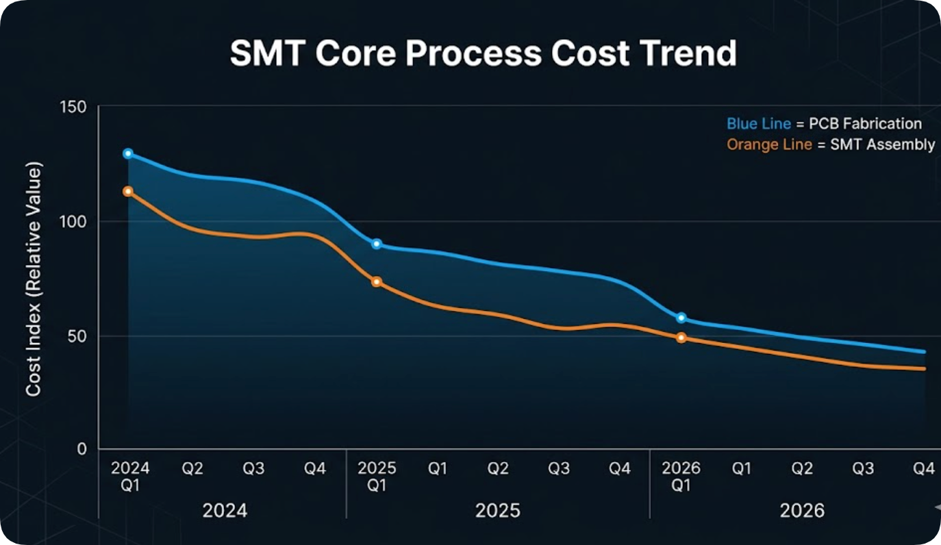
Cost Trends and Supply Chain Insights Affecting SMT Core Processes
The cost of PCB fabrication has risen approximately 8-12% over the last two years due to copper laminate price increases and tighter environmental regulations in China. At the same time, component lead times for certain ICs and passives remain volatile. In my view, the best hedge against these fluctuations is to invest in a robust SMT core process that minimizes waste and rework. Every defective board that passes through rework not only adds cost but also risks damaging adjacent components due to additional thermal stress.
NEWEI addresses these challenges by maintaining strong relationships with multiple substrate suppliers and stocking commonly used components in their own warehouse. This allows the SMT line to run continuously without material shortages, which directly benefits customers who need consistent delivery schedules.
Quality Assurance Beyond the SMT Line
While the SMT core process is the heart of PCBA manufacturing, the surrounding quality assurance steps are equally critical. After reflow soldering, every board passes through Automated Optical Inspection (AOI) to detect missing components, polarity errors, and solder defects. For hidden solder joints under BGAs or QFNs, X-Ray inspection provides the necessary visibility. At NEWEI, these inspections are not just checkpoints—they feed data back to the SMT line to adjust paste volume or placement pressure in real time.
I have personally seen how this closed-loop system reduces defect rates below 50 parts per million, even for complex mixed-technology boards that combine SMT and through-hole components. The Quick Sampling of PCB Circuit Boards service allows customers to validate these quality levels before committing to high-volume production.
Conclusion: Making the Right Technology Partner Choice
The evolution of SMT core processes is not slowing down. As component sizes shrink and performance demands increase, the gap between average and excellent assembly partners will widen. My advice is to evaluate your EMS provider not just on price, but on their ability to adapt new inspection technologies, manage multi-product lines, and provide end-to-end services from PCB fabrication to final assembly and testing.
Whether you are developing an industrial PC, a rugged tablet, or a smart IoT device, working with a partner like NEWEI that invests in advanced SMT processes and integrated service offerings will save you time, money, and headaches. Contact the team today for a free consultation and quotation, and see how their ISO-certified manufacturing can support your next project from prototype to mass production with worldwide shipping and dedicated project manager support.
Tags: SMT process / PCB fabrication / PCBA / evolution / electronics /
Prev: How NEWEI Ensures Delivery Quality for Projector and Rugged Tablet Production
Next: Why HDI Multilayer PCB Capability Defines Your Industrial Motherboard & Mini PC Success


 circuit board testing methods")