How High-Speed SMT, SPI & Wave Soldering Achieve Reliable 0201 and BGA PCB Assembly in Modern Electronics Manufacturing
My View: I’ve visited dozens of SMT factories across Asia over the past decade, from small prototype workshops to fully automated automotive PCBA plants. One thing became obvious very quickly: world-class SMT manufacturing is not defined by flashy machines alone. Anyone can buy a high-speed placement system. What separates reliable factories from unstable ones is process discipline — solder paste consistency, SPI data analysis, thermal profiling, feeder calibration, and how seriously operators treat every micron of alignment. A single 01005 tombstone or a hidden BGA void can quietly destroy an entire product’s reliability months later in the field. That’s why the real story of modern SMT assembly starts long before the first component is placed, and continues well after reflow soldering is complete.
How High-Speed SMT, SPI & Wave Soldering Achieve Reliable 0201 and BGA PCB Assembly in Modern Electronics Manufacturing
By NEWEI Industrial · Advanced SMT Manufacturing Insights · May 2026
The global electronics industry is moving toward smaller, denser, and more complex PCB designs every year. Automotive radar systems, AI edge devices, industrial controllers, smart medical products, and high-speed communication hardware now rely heavily on ultra-compact passive components, fine-pitch ICs, and high-reliability BGA packages. As a result, the demand for precision SMT assembly, 3D SPI inspection, high-speed pick-and-place manufacturing, and wave soldering process control continues to rise globally.
According to industry forecasts, the global SMT equipment market is expected to exceed $6.2 billion by 2027, largely driven by miniaturized electronics and the rapid growth of automotive PCBA production. However, achieving stable yields with 0201 components, 0.35mm CSP packages, and complex BGA soldering requires far more than simply purchasing advanced equipment.
At NEWEI Industrial, our production floor combines high-speed SMT placement lines, inline SPI inspection, AOI verification, DIP insertion, and nitrogen-assisted wave soldering into one tightly controlled manufacturing ecosystem. Every stage is connected through MES traceability and monitored in real time. This article walks through the actual production workflow behind reliable, high-density PCB assembly.
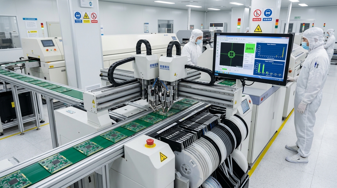
Fig 1 – High-speed SMT line running at full capacity: dual independent placement heads mounting 0201 passives and fine-pitch ICs simultaneously.
⚙️ High-Speed SMT Placement – Precision Beyond Raw Speed
Modern SMT manufacturing is often marketed using placement speed numbers alone — 40k, 60k, or even 100k CPH. In reality, pure speed means very little if placement stability and repeatability are inconsistent. Our production lines use dual-beam, dual-gantry placement systems capable of processing more than 45,000 components per hour while maintaining micron-level accuracy.
Each placement head uses independent vision correction before every critical placement. Component polarity, lead coplanarity, offset angle, and pickup integrity are verified in milliseconds. If a feeder begins showing abnormal pickup behavior, the system immediately flags it for operator inspection before defects spread across an entire production batch.
For automotive radar PCBs containing more than 4,000 placements per board, maintaining placement consistency is essential. Over the last six months, our SMT lines maintained a verified placement accuracy of ±25μm for micro passive devices, supporting stable yields even on high-density multilayer assemblies.
The most challenging products are not always the largest boards. Often, compact IoT or wearable products containing hundreds of 0201 or 01005 components require even tighter process control because there is almost no physical margin for solder movement during reflow.
🖨️ Solder Paste Printing and SPI – The Real Foundation of SMT Quality
In professional SMT manufacturing, solder paste printing is often considered the single most important process step. Poor paste deposition leads directly to insufficient solder joints, bridging, tombstoning, and hidden reliability failures. Even the world’s fastest placement machine cannot compensate for unstable solder paste volume.
Our stencil printing process uses laser-cut stainless steel stencils combined with controlled squeegee pressure, automatic stencil underside cleaning, and closed-loop alignment verification. Environmental temperature and humidity are monitored continuously because solder paste viscosity changes significantly under unstable conditions.
Immediately after printing, every PCB enters our 3D SPI inspection system. This stage measures solder paste height, volume, offset, and shape using high-resolution optical scanning.

Fig 2 – 3D SPI analysis: color-coded solder paste height map for a fine-pitch QFN pad array.
Boards exceeding preset tolerance thresholds are automatically rejected before entering placement. This proactive process prevents downstream defects and dramatically reduces rework costs. Since implementing full inline SPI verification, solder-related DPPM levels on several industrial product lines have decreased substantially.
Process engineers also use SPI trend data to monitor stencil wear, cleaning efficiency, and paste aging over long production runs. Instead of reacting to defects after reflow, we focus on preventing instability before assembly even begins.
🧩 0201 Placement and BGA Soldering – Where Precision Becomes Critical
0201 SMT assembly demands extremely careful process tuning. These tiny components measure only 0.6 × 0.3mm, making them highly sensitive to placement force, solder balance, and thermal variation. Even small nozzle contamination can affect alignment accuracy.
To improve reliability, our SMT lines dedicate specific placement heads to micro passive components. Pickup force, nozzle vacuum pressure, and placement height are adjusted specifically for ultra-small packages. Nozzles are cleaned regularly to reduce static adhesion and component flipping.
BGA assembly presents an entirely different challenge. Unlike visible solder joints, BGA balls are hidden beneath the package, making defects difficult to identify without X-ray inspection. Thermal balance during reflow becomes extremely important because uneven heating may cause head-in-pillow defects, voiding, or incomplete wetting.
Every high-reliability BGA product undergoes X-ray sampling inspection. Reflow profiles are optimized using thermal data collection across multiple board locations to ensure uniform solder wetting behavior. Our process engineering team continuously fine-tunes soak time, ramp rate, and peak temperature to minimize solder stress while maintaining stable joint formation.
For automotive and industrial applications, stable BGA solder integrity is far more important than simply passing AOI inspection. Long-term thermal cycling reliability must also be considered during process development.
🔌 DIP Assembly and Wave Soldering Still Matter in Modern Electronics
Although SMT dominates modern PCB manufacturing, DIP insertion and wave soldering remain essential for connectors, transformers, power modules, and mechanically stressed components. Through-hole solder joints often handle higher electrical and mechanical loads than surface-mount devices.
After SMT reflow is complete, boards move into our controlled DIP assembly area where operators follow digital work instructions displayed on ESD-protected terminals. Barcode verification helps prevent component mismatch during manual insertion.
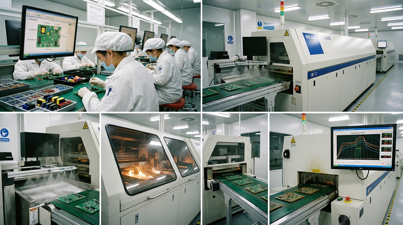
Fig 3 – DIP insertion and selective wave soldering process with nitrogen-assisted protection.
Our wave soldering systems use controlled flux management, programmable conveyor speed, and nitrogen-assisted solder protection to improve joint consistency. Parameters including solder pot temperature, preheat curve, and conveyor angle are logged continuously for process traceability.
By analyzing historical wave soldering data, process engineers can identify trends long before defects become statistically significant. This data-driven approach has helped reduce solder bridging and improve final electrical testing performance across multiple industrial PCBA projects.
📈 Real-Time MES Traceability from SMT to Final Assembly
One of the biggest differences between conventional factories and advanced electronics manufacturing facilities is traceability integration. At NEWEI, every PCB receives a unique barcode at the beginning of production. The MES system records paste inspection data, placement history, feeder usage, thermal profile logs, AOI inspection results, and wave soldering parameters for every board.
If a customer reports an issue months later, engineers can quickly retrieve the complete manufacturing history of the exact PCB involved. This level of transparency is increasingly important for automotive electronics, industrial control systems, smart energy products, and medical devices.
Modern SMT manufacturing is no longer simply about machines assembling components. It is about building a fully connected, data-driven production ecosystem where every process can be monitored, analyzed, optimized, and traced in real time.
Final Thought: Reliable PCB assembly is never the result of one machine or one inspection step. It comes from disciplined control over every stage — solder paste printing, SPI verification, SMT placement, reflow profiling, DIP insertion, and wave soldering. At NEWEI Industrial, every solder joint is treated as part of a larger reliability system designed for long-term field performance.
📞 Contact NEWEI Industrial
Tel: +86-18925218989
Email: tiger.wang@richitek.com
Web: https://www.neweiodm.com/
Request a live SMT production audit or submit your BOM for manufacturing capability evaluation.
©2026 NEWEI Industrial – Precision SMT, SPI, BGA and wave soldering solutions for advanced electronics manufacturing.
Tags: SMT assembly / 3D SPI inspection / 0201 micro‑placement / wave soldering process /
Next: Mastering PCBA Quality Control: Why 3D AOI, X-Ray, ICT/FCT, and Full Traceability are Non-Negotiable