How a Handheld Gaming (PSP) OEM Achieved First‑Article Pass & Smooth Mass Production with NEWEI‘s Custom PCB Assembly Services
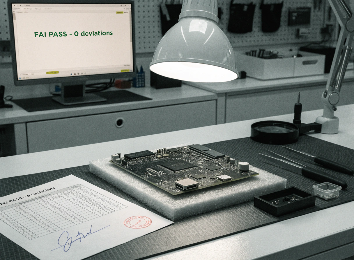
Fig 1 – First article inspection (FAI) of the PSP gaming mainboard: all electrical and mechanical tests passed on first submission
My View: In the handheld gaming industry, time‑to‑market is measured in weeks, not months. A single engineering change order can push a product launch past the holiday window. That‘s why the trust of a gaming OEM is one of the hardest things to earn – and the most rewarding to keep. When a leading brand in the PSP (portable gaming console) space came to us with a complex, high‑density mainboard design, they had one request: first‑article pass on the first try, and a clear path to 50k units per month. This article tells the story of how our DFM, SMT, and test engineering teams delivered exactly that – and why the client now considers us a strategic partner, not just a supplier.
How a Handheld Gaming (PSP) OEM Achieved First‑Article Pass & Smooth Mass Production with NEWEI‘s Custom PCB Assembly Services
By NEWEI Industrial · May 2026 · 12 min read
The global handheld gaming console market is expanding rapidly, driven by a surge in premium retro-inspired portable hardware and cloud-enabled high-performance devices. Unlike standard consumer electronics, modern gaming handhelds pack massive computational power into tight ergonomics. This requires dense component layouts, high-speed signal integrity, and impeccable thermal management. For original equipment manufacturers (OEMs), engineering a flawless launch means bypassing the common manufacturing pitfalls that cause delayed product rollouts and component damage.
To secure a reliable production pipeline, electronics brands depend on experienced Custom PCB Assembly Services that bridge the gap between design files and high-yield mass manufacturing. When a top-tier portable gaming brand approached NEWEI with an intricate, ultra-dense mainboard layout, they needed more than an electronics manufacturing services (EMS) vendor; they required a strategic turnkey partner. This case study details how our integrated Design for Manufacturability (DFM) assessment, automated surface-mount technology (SMT) lines, and thorough First Article Inspection (FAI) achieved a 100% initial pass rate and unlocked a scalable path to 50,000 units per month.
🎮 1. The Challenge – High‑Density PSP Mainboard with Mixed Technology
The client's hardware layout presented an engineering bottleneck. The core motherboard measured just 85×55mm but contained more than 800 individual components packed into a multi-layer stack-up. Central to the device was a ultra-fine 0.35mm-pitch system-on-chip (SoC) application processor, flanked closely by high-speed LPDDR4X memory modules, eMMC storage, and an integrated power management integrated circuit (PMIC). Furthermore, the peripheral layout included sensitive RF front-end circuitry for dual-band Wi-Fi and Bluetooth, requiring strict trace isolation and shield grounding.
Because portable devices are exposed to variable environmental factors, the client's engineering specification mandated selective conformal coating across moisture-sensitive zones to prevent damage from sweat, humidity, and dust. Before auditing NEWEI, the client had engaged two separate contract manufacturers. Both suppliers failed to maintain stable yields, suffering from recurring Ball Grid Array (BGA) bridging, high voiding percentages, and an overall SMT first-pass yield hovering below 92%. With an upcoming Q4 retail window, the client came to us with strict operational KPIs:
- An unconditional First-Article Inspection (FAI) pass with zero layout deviations.
- An SMT first-pass yield (FPY) exceeding 98.5% across all production lots.
- A fully verified production ramp-up reaching 50,000 units per month within a 90-day window.
🛠️ 2. Our Solution – DFM Optimization, Process Validation, and Rigorous Testing
Our New Product Introduction (NPI) team initiated a deep-dive Design for Manufacturability (DFM) evaluation before setting up the SMT line. Analyzing the Gerber files, our engineers identified three critical design vulnerabilities that would have compromised industrial-scale yields:
Solder Mask Dam Optimization: The native BGA land pattern lacked adequate solder mask dams between the fine-pitch pads, exposing the assembly to solder bridging during reflow. We modified the solder mask apertures to establish a reliable, stable barrier between adjacent solder spheres.
Thermal Pad Segmentation: The large, continuous thermal ground pad under the main PMIC lacked appropriate gas venting channels. During reflow, outgassing from flux would inevitably get trapped, creating internal voiding. NEWEI redesigned the paste stencil to segment the pad into an optimized windowpane matrix, providing reliable escape paths for volatile gases.
Tombstoning Mitigation: The original distance between the mechanical RF shield solder joints and small 0201 passive components was uneven. This caused unbalanced thermal absorption, pulling the smaller components upright. We adjusted the pad geometry and local trace dimensions to ensure uniform thermal distribution during the heating cycle.
Once the client signed off on these DFM improvements, we initiated a controlled pre-production run of 10 validation boards. Our manufacturing team utilized precision electroformed stencils with an optimized 0.75 area ratio to control paste deposition volumes. We customized the reflow oven profile, extending the soak stage to 100 seconds to equalize temperatures across the high-mass SoC and low-mass passives, and integrated a vacuum-assisted reflow phase. High-resolution 3D Automated Optical Inspection (AOI) confirmed an excellent SMT first-pass yield of 99.3%, with automated X-ray inspection (AXI) verifying that the BGA internal voiding area averaged a mere 12%—far safer than the industry-standard 20% limit.
Fig 1 – First article inspection (FAI) of the PSP gaming mainboard: all electrical and mechanical tests passed on first submission

Fig 2 – Pilot run of 500 PSP mainboards: SMT placement, selective conformal coating, and functional test stations
✅ 3. First‑Article Inspection (FAI) – One‑Shot Approval
With engineering validations complete, we built a formal five-board First Article batch using our automated FAI measurement system. Instead of relying on manual spot checks, our digital inspection system maps the physical board directly against the primary BOM and CAD coordinates, checking every component value, orientation, and placement placement within seconds.
NEWEI delivered a comprehensive engineering quality documentation package alongside the physical samples, providing the client's quality assurance team with total clarity:
- 3D AOI Micro-Images: High-resolution, multi-angle physical layout documentation of every single component joint.
- AXI Voiding Analysis: Comprehensive X-ray structural reports detailing internal solder density across all hidden BGA and QFN interfaces.
- In-Circuit Testing (ICT) Logs: Complete electrical parametric data ensuring zero opens, shorts, or passive out-of-tolerance values.
- Full Functional Testing (FCT): Component-level firmware verification validating core booting sequences, memory write/read operations, I/O performance, and wireless RF signal-to-noise ratios.
- Precision Conformal Coating Mapping: Micro-thickness gauge validations collected across five separate high-risk zones per module to guarantee insulation consistency.
- Laser Dimensional Auditing: Full physical metrology reports confirming tight compliance across critical mounting hole tolerances and edge clearances.
The client's incoming quality control team evaluated our FAI submission and issued a formal approval with zero deviations. By executing the transition correctly from the first build, we saved the client weeks of diagnostic debugging and prevented costly stencil re-tooling charges.
📈 4. Pilot Run to Mass Production – Scaling to 50k Units per Month
Following the FAI milestone, we initiated a 500-unit pilot production run to analyze operational efficiency and ensure long-term stability under high-speed manufacturing conditions. It was during this phase that our component quality engineering (CQE) team demonstrated the true value of an experienced manufacturing partner. We caught an intermittent coplanarity flaw within an incoming batch of external touch-panel ribbon connectors. The variable seating height threatened to create cold solder joints during reflow.
Instead of halting production, we instantly isolated the non-conforming batch, notified the customer's engineering team, and worked with our verified vendor network to source an alternate component. Our proactive response saved the client from what could have evolved into an expensive field-failure issue. The pilot run concluded with a first-pass yield of 97.6%, which rose to a final yield of 99.8% after automated rework.
With process controls locked down, wescaled production output to 50,000 units monthly within just 10 weeks—beating the client's original timeline by two full weeks. Our dedicated assembly facility operates on a two-shift schedule, fully backed by online 3D SPI, 3D AOI, continuous X-ray monitoring, and automated ICT/FCT fixtures. Long-term production data shows our defect rate has stabilized below 800 DPPM, setting a new benchmark for gaming hardware production.

Fig 3 – Customer audit team inspecting PSP mainboard aging test process; mass production contract signing
🤝 5. Customer Success – From Pilot to Long‑Term Partnership
Six months after launching high-volume production, the client sent an international quality auditing team to our manufacturing plant for a comprehensive review of our quality management systems and component traceability. Over two full days, the audit scrutinized our incoming material controls (IQC), real-time SPI/AOI monitoring records, defect Pareto tracking charts, and first-in, first-out (FIFO) inventory systems.
The audit concluded with zero major non-conformances, prompting the client to upgrade NEWEI to their coveted "Preferred Manufacturing Partner" rank. Since that successful audit, we have been awarded contract extensions for two next-generation portable gaming platforms, pushing our total cumulative production beyond 300,000 units. Furthermore, the client's logistics team has referred two additional gaming peripheral brands to NEWEI, both of which are now moving through our NPI validation process.
📊 Key Metrics from the PSP Program
- First-Article Inspection (FAI) Pass Rate: 100% on the very first submission.
- SMT First-Pass Yield (Pilot Phase): 97.6% across pre-production runs.
- SMT First-Pass Yield (Mass Production): Sustained at 98.9% over high-volume lots.
- Average BGA Solder Voiding: Maintained at 12% (well within the client's ≤20% requirement).
- 6-Month Field Return Rate: Only 0.18% (compared to the typical industry average of 0.6%).
- On-Time Delivery (OTD) Performance: Perfect 100% shipping record over a 12-month period.
- Product Lifecycle Extensions: Secured 2 additional long-term contracts for next-gen models.
Partner with an Elite PCBA Manufacturer
Industrial excellence is built step by step—from initial DFM reviews to final product delivery. At NEWEI, we combine technical manufacturing precision with advanced turnkey capabilities to support your most demanding projects. The success of this high-density handheld gaming console program demonstrates how our end-to-end oversight mitigates risks and scales production seamlessly.
📞 Contact NEWEI (Newei Industrial)
Tel: +86-18925218989
Email: tiger.wang@richitek.com
Web: https://www.neweiodm.com
Reach out to our engineering team today to upload your Gerber files for a complimentary DFM analysis, or explore our flexible Custom PCB Assembly Services tailored to high-performance consumer hardware.
©2026 NEWEI Industrial – From first‑article to million‑unit production, we deliver.
Tags: Handheld gaming PCBA one‑stop service / PSP mainboard first‑article pass /