How X‑RAY, ICT/FCT & Quality Traceability Deliver Zero‑Defect Rugged Tablet PCBA – A Complete Testing Workflow
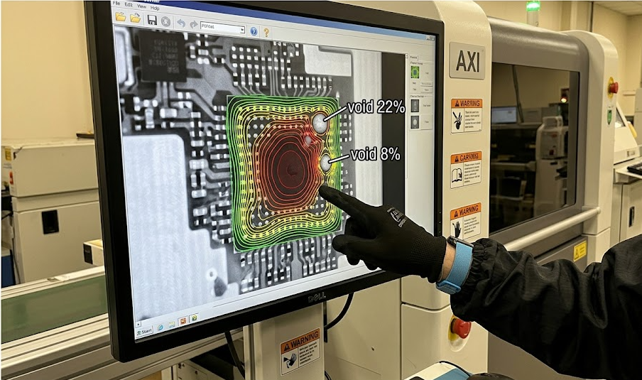
Fig 1 – X‑RAY inspection of a rugged tablet PCBA: real‑time void detection under BGA and QFN packages
My View: For rugged tablets deployed in harsh field service, heavy logistics, and unpredictable outdoor operations, a single hidden BGA void or a microscopic cold solder joint will inevitably transform a mission‑critical enterprise device into an expensive brick. While standard Automated Optical Inspection (AOI) catches superficial defects, X-RAY penetrates deep to expose hidden joint anomalies, and ICT/FCT validates performance under actual electrical stress. True quality control requires a multi‑stage hardware validation workflow tied to real-time manufacturing execution systems. At NEWEI, zero‑defect output is an actively enforced engineering methodology, ensuring every hardware batch survives the toughest industrial field conditions.
How X‑RAY, ICT/FCT & Quality Traceability Deliver Zero‑Defect Rugged Tablet PCBA – A Complete Testing Workflow
By NEWEI Industrial · May 2026 · 12 min read
The global industrial rugged tablet market is accelerating rapidly, driven by the digital transformation of field logistics, public safety infrastructure, and smart warehouse management. Unlike standard consumer electronics, rugged hardware must withstand repeated drops, continuous mechanical vibrations, extreme thermal shock, and high moisture ingress. This demanding environment means that a latent solder defect hidden underneath a high-density Ball Grid Array (BGA) package or a minor patch of insufficient conformal coating will trigger hardware failure within months of deployment. To eliminate early field failures, high-reliability electronics factories rely on comprehensive Custom PCB Assembly Services that integrate advanced inspection technologies. Our manufacturing ecosystem for rugged devices uses a rigorous multi-layer quality gate sequence: high-resolution 3D AOI, Automated X-ray Inspection (AXI), In-Circuit Testing (ICT), Functional Testing (FCT), active shop-floor patrol QC, comprehensive first-article verification, and full-lifecycle MES defect traceability. This deeply integrated testing framework maintains strict Defective Parts Per Million (DPPM) control across large-scale industrial manufacturing runs.
🔬 1. 3D AOI & X‑RAY Inspection – Exposing Both Surface and Hidden Solder Anomalies
Immediately following the reflow soldering stage, every rugged tablet mainboard enters an automated, inline 3D AOI (Automated Optical Inspection) system. Utilizing multi-frequency digital fringe projection, the 3D AOI calculates true component heights, volumetric solder fillet geometries, and precise lead coplanarity. This layer catches surface-level placement defects, including lifted leads, component tombstoning, bridge shorts, and skewed chips. Trained on an extensive library of industrial defect signatures, our AOI systems achieve a remarkably low false-call rate below 0.8% while capturing 99.5% of true surface anomalies.
However, optical systems cannot inspect joints hidden beneath high-density BGAs, QFNs, or metallic RF shielding cans. For these critical areas, Automated X-ray Inspection (AXI) serves as an essential quality gate. Operating with a high-resolution micro-focus tube (5–8 µm focal spot size) and multi-axis manipulators that tilt the circuit board up to 70 degrees, our X-ray inspection equipment captures distinct oblique views. This radiography technique measures volumetric voiding percentages, detects subtle head-in-pillow (HiP) defects, and confirms true solder wetting across hidden pads. For industrial and automotive-grade rugged electronics, we enforce a strict interior voiding limit of ≤20% across all BGA balls—a standard tighter than the conventional IPC-A-610 Class III threshold of ≤25%. Any joint exceeding this parameter automatically triggers a manufacturing halt for that specific serial number, and the high-resolution radiographic imaging data is instantly appended to the Manufacturing Execution System (MES) log for permanent tracking.
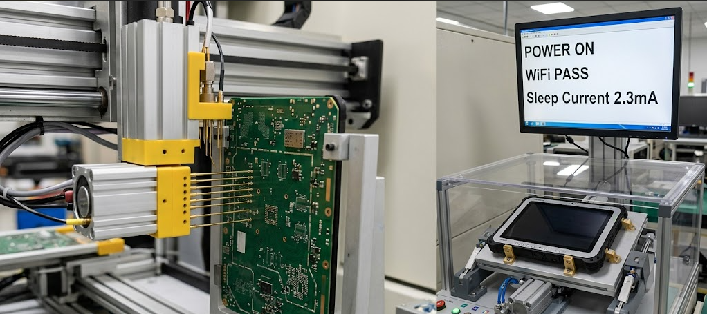
Fig 2 – ICT (left) and custom FCT fixture (right) for rugged tablet: testing power rails, I/O, and wireless modules
⚡ 2. ICT & FCT – Verifying Electrical Integrity and Full Operational Performance
Optical and radiographic validation processes confirm mechanical structural integrity, but they cannot verify that the device operates perfectly under real-world electrical loads. Therefore, we utilize specialized In-Circuit Testing (ICT) and Functional Testing (FCT) as our primary electrical verification barriers. For high-density rugged tablet PCBAs, our flying probe or custom bed-of-nails ICT units check for short circuits, open traces, precise passive component values (including resistance, capacitance, and inductance), and proper component orientation. This diagnostic step runs entirely unpowered, protecting sensitive silicon from voltage exposure if a manufacturing short exists. For high-volume industrial projects, automated multi-up ICT fixtures test up to four mainboards simultaneously, multiplying production throughput while achieving over 98% component fault coverage.
Once a board clears the unpowered ICT stage, it advances directly to our custom-engineered Functional Testing (FCT) stations. These intelligent testing jigs simulate actual field use by applying precise battery emulation voltages, monitoring complex power-up timing loops, and measuring current draw down to micro-amp levels in deep sleep modes. Specialized coaxial RF switches route signals to verify cellular, Wi-Fi, GPS, and Bluetooth transmission paths, while specialized automated tests check the screen backlight power, touch matrix responses, and digital peripheral inputs. Our real-world data demonstrates an average FCT first-pass yield of 97.8% on recent rugged platform builds, with comprehensive diagnostic feedback loops driving our post-rework final yield up to a verified 99.7% before final casing assembly.
📋 3. Patrol QC & First‑Article Verification – Maintaining Strict Standardized Floor Control
While automated testing machinery provides unmatched speed and detail, human engineering oversight remains vital to long-term quality consistency. Our dedicated quality assurance teams execute hourly floor patrol audits across the entire SMT and assembly line. These audits inspect critical processing variables, including solder paste viscosity, laser stencil cleanliness, reflow oven thermal profile drift, and active Electrostatic Discharge (ESD) grounding integrity. Every single checkpoint measurement is updated instantly into our factory MES via rugged mobile devices, meaning any processing non-conformance immediately pauses production before defective units can accumulate.
Furthermore, before starting any new production run, we execute a meticulous First Article Inspection (FAI) protocol on the initial five completed boards. The FAI process utilizes advanced vision measurement systems and digital calipers to check mechanical dimensions, followed by detailed 3D AOI, X-ray inspection, and comprehensive ICT/FCT electrical charting. A complete, itemized FAI quality report is provided directly to the client for validation and sign-off before mass production begins. This preemptive validation cycle acts as a vital shield against manufacturing errors; for instance, it previously caught an out-of-spec passive component variance from a third-party supplier, allowing immediate correction before an entire 1,000-unit batch could be assembled. Thanks to these strict pre-flight procedures, our initial production runs have maintained an unblemished zero-rejection track record for over 18 consecutive months.
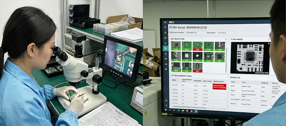
Fig 3 – Defect analysis lab (left) and MES traceability portal (right): linking field failures to specific inspection gates
🔁 4. Root‑Cause Defect Analysis & Full MES Traceability – Closing the Quality Loop
Even with advanced, multi-tiered inspection checkpoints, an occasional hidden material variance can emerge during final testing stress runs. When an anomaly is detected, our on-site failure analysis laboratory executes an immediate root-cause investigation. Technicians utilize metallographic cross-sectioning, high-magnification microscopes, digital curve tracers, and diagnostic X-ray targeting to isolate the failure mechanism. Within 24 hours of any test failure, our engineering department delivers a comprehensive 8D problem-solving report, precisely detailing the root cause—such as localized solder bridging from paste shelf-life limits or micro-voiding caused by specialized reflow profile adjustments. Our long-term tracking classifies manufacturing defect distributions into clear target areas: solder bridge shorts (34%), BGA voiding anomalies (28%), passive component tombstoning (18%), insufficient paste volume (12%), and component placement offset (8%).
All of this diagnostic data flows directly into our integrated MES traceability portal. Every single circuit board receives a unique, laser-etched 2D data-matrix code that tracks its entire life history through the plant. This code records component lot numbers, placement machine identifier codes, exact thermal reflow profiles, raw 3D AOI data, high-resolution X-ray images, precise ICT/FCT logs, and any technician rework histories. If a rugged tablet experiences a field failure years after delivery, our quality management team can trace the hardware back to its exact component supplier lot, production shift, and specific manufacturing station within minutes. This reliable, data-backed transparency provides enterprise clients with absolute peace of mind and has proven vital when securing long-term supply agreements for aerospace, heavy logistics, and defense-related equipment. Over the last two years, our internal data-driven engineering refinements have slashed our overall assembly DPPM by 47%, successfully elevating final testing pass rates beyond 99.6%.
📊 Key Operational Quality Metrics – Real‑Time Factory Performance
- AOI First-Pass Yield: 96.3% on high-density industrial tablet lines.
- Automated X-Ray Rejection Rate: 0.9% (systems instantly isolate voids >20%).
- ICT First-Pass Success Rate: 98.1% (including automated false-call adjustments).
- FCT Final Yield Metrics: 99.6% verified pass rate following automated post-rework testing loops.
- Average 8D Engineering Resolution: Complete root-cause reporting and system closure within 22 hours.
- Traceable Manufacturing Data Points: More than 2,000 distinct records preserved per board, spanning material receipt to secure final packaging.
Your Rugged Tablet's Long-Term Field Reliability is the Result of Rigid Process Control
At NEWEI, we treat product quality as an active engineering discipline rather than a final checklist. By conducting X-ray imaging on every BGA, functional testing on every system circuit, and tracking every single step via MES, we guarantee your industrial hardware survives the elements.
📞 Contact NEWEI (Newei Industrial) to Discuss Your Next Project:
Tel: +86-18925218989
Email: tiger.wang@richitek.com
Official Web Portal: https://www.neweiodm.com
Reach out today to coordinate a comprehensive factory quality audit or to evaluate real X-ray, ICT, and FCT data sets for your upcoming rugged device deployment.
©2026 NEWEI Industrial – From AOI to AXI, ICT, FCT, and complete MES traceability: every board, every test, every historical record preserved.
Tags: Rugged tablet PCBA inspection / X‑RAY BGA void detection /